Semiconductor Foundry Market Size & Forecasts 2026-2035, By Segments (Technology Nodes, Foundry Type, Application), Growth Opportunities, Innovation Landscape, Regulatory Shifts, Strategic Regional Insights (U.S., Japan, China, South Korea, UK, Germany, France), and Competitive Dynamics (TSMC, Samsung Electronics, GlobalFoundries, UMC, SMIC)
Market Size and Growth Outlook
Semiconductor Foundry Market size is expected to advance from USD 60.96 billion in 2025 to USD 130.39 billion by 2035, registering a CAGR of more than 7.9% across 2026-2035. By 2026, the industry is anticipated to generate USD 65.18 billion in revenue.
Get more details on this report
Request Free Sample ReportSemiconductor Foundry Market Intelligence Snapshot
Regional Market Dynamics
Segment Momentum
Market Expansion Drivers
Leading Market Participants
Global Market Forecast Snapshot
Market Outlook
Regional and Segment Outlook
Market Growth Drivers and Industry Trends
Technological advancements in wafer fabrication and lithography: Breakthroughs in EUV and metrology capabilities are reshaping cost and capability trade-offs across the semiconductor foundry market; ASML’s EUV systems (and High-NA development) plus Applied Materials’ and KLA’s equipment roadmaps, reinforced by imec research collaborations, demonstrate how toolchain evolution enables finer geometries and yield improvements. Foundries that integrate next-generation lithography and advanced process control capture higher-value workloads, while startups can enter by offering specialized process modules, IP or advanced packaging stacks. The visible progress from ASML, Applied Materials and research hubs points to an accelerated cadence of node enablement tied to equipment availability.
Expansion of foundry services for automotive and IoT applications: Growth in vehicle electrification, ADAS and pervasive sensors expands addressable demand in the semiconductor foundry market, prompting suppliers to pursue automotive qualifications and IoT-focused offerings; GlobalFoundries and TSMC have publicized automotive-qualified processes and partnerships, while NXP Semiconductors and Qualcomm continue to announce automotive SoC programs that rely on qualified foundry capacity. This creates strategic options for established foundries to monetize certification and functional-safety ecosystems and for new entrants to target low-power, secure IoT nodes and system-in-package services. Ongoing public certifications and OEM design wins indicate durable segmentation of foundry services toward automotive and IoT use cases.
Industry Restraints:
Geopolitical Export Controls and Trade Restrictions
Export controls and trade restrictions are a major choke point that slows technology diffusion and raises compliance and re‑engineering costs across the foundry ecosystem. The U.S. Department of Commerce’s Entity List actions and licensing regimes have constrained sales of advanced process technologies and inputs to targeted firms, while ASML has publicly cited adherence to Dutch export controls that limit EUV shipments to mainland China. These measures increase legal and logistical burdens for global supply chains, fragment end markets, and impede collaboration between partners. For incumbents such as TSMC and Samsung the result is re‑sourcing and regional capacity builds; for challengers like SMIC the effect is delayed node advancement and higher unit costs. Expect continued regulatory-driven regionalization over the near to medium term, with firms adapting via localized fabs, more rigorous compliance functions, and bilateral supplier networks.
Capital Intensity and Concentration of Advanced Tool Suppliers
The extreme capital outlay and the bottleneck in critical equipment constrain scale-up cadence and raise barriers to entry. ASML’s EUV systems remain scarce and costly, and ASML has reported multi‑year delivery backlogs; SEMI equipment data and public statements from TSMC and Intel describing multibillion‑dollar fab expansions underscore persistent demand for high‑end tools and fabs. This concentration favors deep‑pocketed incumbents who can prepay, secure long lead items, and amortize R&D, while new entrants and regional players face deferred ramp-up or must pursue older nodes. Strategically, market players will pursue partnerships, government subsidy programs, and captive supply agreements to mitigate risk. Over the next several years this capital‑and‑supplier concentration will sustain consolidation around leading foundries and catalyze closer public‑private investment coordination.
| Growth Driver | Impact on CAGR | Regulatory Influence | Geographic Relevance | Adoption Rate | Impact Timeline |
|---|---|---|---|---|---|
| Increasing demand for advanced semiconductor devices | 3.00% | Short term (≤ 2 yrs) | North America, Asia Pacific | Medium | Fast |
| Technological advancements in wafer fabrication and lithography | 2.50% | Medium term (2–5 yrs) | Europe, North America | Medium | Moderate |
| Expansion of foundry services for automotive and IoT applications | 2.40% | Long term (5+ yrs) | Asia Pacific, Europe; Spillover: North America | Low | Slow |
Unlock insights tailored to your business with our bespoke market research solutions.
Click to get your customized report now.
Regional Demand Dynamics
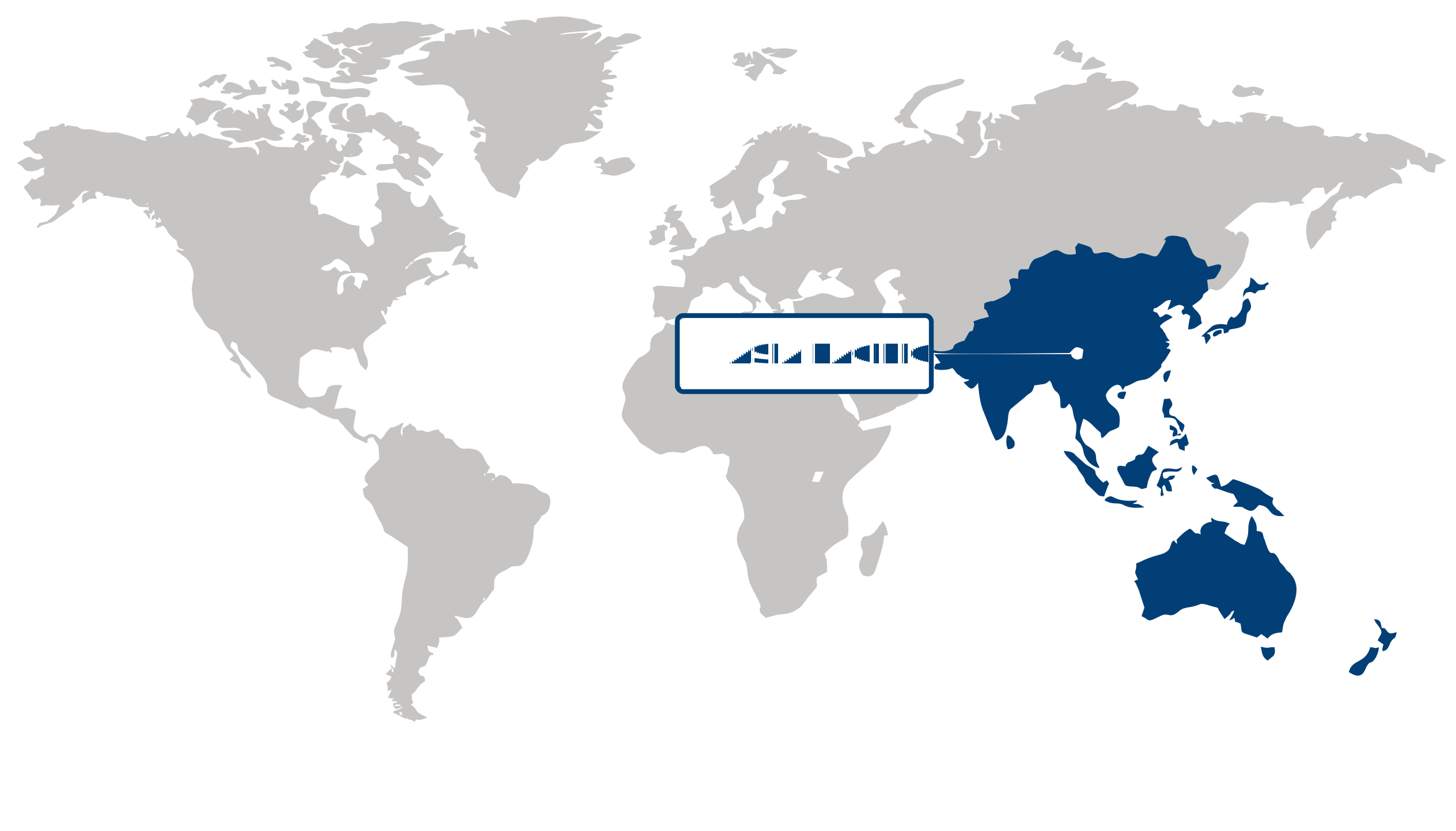
semiconductor foundry market captured about 68% of the global market in 2025, making Asia Pacific the largest regional hub by share, driven by a robust manufacturing ecosystem and strong government support. Evidence includes Taiwan Semiconductor Manufacturing Company (TSMC) capacity expansion announcements and Samsung Electronics’ advanced-node investments alongside policy actions from the Ministry of Industry and Information Technology (MIIT) and financing by the China National Integrated Circuit Industry Investment Fund. Deep supplier bases—illustrated by Tokyo Electron Limited and Shin‑Etsu Chemical—and coordinated public programs shorten lead times, enable node progression for AI and automotive workloads, and improve sustainability and operational resilience. These structural strengths mean Asia Pacific is well positioned to capture differentiated demand for specialized nodes and localized, low-carbon production solutions.
semiconductor foundry market Japan is positioned as a pivotal hub in Asia Pacific for materials, equipment and niche fabs, supported by targeted public initiatives. The Ministry of Economy, Trade and Industry (METI) has promoted capital and workforce programs while Tokyo Electron Limited and Shin‑Etsu Chemical signal supply-chain commitments that reinforce advanced packaging and legacy-node capacity for automotive and industrial customers. This specialization reduces regional bottlenecks and complements high-volume capacity in neighboring markets, making Japan a strategic partner for capacity diversification across Asia Pacific.
semiconductor foundry market China anchors volume expansion in Asia Pacific through scale-driven capacity growth and state-backed finance and policy. The China National Integrated Circuit Industry Investment Fund and guidance from the Ministry of Industry and Information Technology (MIIT) underpin Semiconductor Manufacturing International Corporation (SMIC) capacity announcements and meet surging domestic OEM demand for smartphones, EVs and AI servers. Localized input sourcing and logistics initiatives under MIIT priorities enhance cost competitiveness and supply security, reinforcing Asia Pacific’s ability to serve global demand across node tiers.
North America Market Analysis:
North America emerged as the fastest-growing region in the semiconductor foundry market, registering a robust CAGR of 9.3% as reshoring strategies and government incentives accelerate onshore capacity and investment. Policy measures such as the CHIPS and Science Act and actions by the White House, together with implementation through the U.S. Department of Commerce CHIPS Program Office, have catalyzed capital deployment and supplier relocation, prompting major announcements from Taiwan Semiconductor Manufacturing Company (TSMC), Intel Corporation, and GlobalFoundries to expand U.S. fabrication capacity. These moves are reshaping supplier networks, tightening links with hyperscalers and automotive OEMs, and driving demand for advanced nodes and reliable domestic supply. Given continuing public funding and private commitments, North America is positioned to capture outsized market share as companies prioritize resilience and proximity to large end markets.
U.S. plays the central role in the semiconductor foundry market for North America, where federal incentives and corporate greenfield projects convert policy into tangible fab capacity. The U.S. Department of Commerce CHIPS Program Office has enabled awards and guidance that de-risk investments cited in press releases from Intel Corporation and Taiwan Semiconductor Manufacturing Company (TSMC); GlobalFoundries’ statements on New York expansion similarly illustrate how state and federal packages translate to build-out. Labor coordination with universities and regional workforce programs is improving skills supply while procurement from cloud providers and automotive manufacturers sustains orders. Strategically, the U.S. hub amplifies regional opportunities by anchoring a resilient, investment-ready ecosystem that attracts both domestic and foreign foundry commitments.
Europe Market Trends:
Maintained notable presence in the semiconductor foundry market, Europe exhibits moderate growth driven by coordinated industrial policy, specialized equipment supply, and a dense cluster of design-to-manufacturing partners. The European Commission’s Chips Act and targeted funding programs have catalyzed capacity-building while ASML’s equipment orders and Infineon Technologies press releases on capacity investments underscore continued upstream and downstream commercial activity. Sustainability priorities and reshoring initiatives are reshaping investment patterns, logistics, and supplier relationships, and companies such as STMicroelectronics have highlighted collaborative roadmaps with research institutes to accelerate process nodes. These dynamics position Europe as an attractive arena for selective capital deployment and strategic partnerships over the medium term.
Germany is a core manufacturing hub in the semiconductor foundry market and is characterized by strong automotive-driven demand and an advanced production ecosystem. Federal Ministry for Economic Affairs and Climate Action statements and Infineon Technologies press releases on facility expansions reflect public–private coordination to scale capacity, while deep engineering talent and localized supply chains support complex mixed-signal and power device fabrication. The concentration of automotive OEMs and Tier‑1 suppliers creates predictable, high-volume demand patterns, making Germany strategically important for investors seeking industrial-scale foundry exposure within Europe.
France plays a leading innovation role in the semiconductor foundry market, leveraging R&D clusters, public finance, and technology transfer to support specialty process development. STMicroelectronics press releases, CEA‑Leti collaborations, and Bpifrance initiatives illustrate how public funding and research infrastructure accelerate pilot lines and IP creation for niche CMOS variants and power devices. Strong university–industry linkages and government-backed commercialization programs favor prototyping and higher-value nodes, making France an ideal complement to Germany’s manufacturing scale and enhancing pan‑European opportunities for differentiated foundry services.
| Parameter | North America | Asia Pacific | Europe | Latin America | MEA |
|---|---|---|---|---|---|
| Innovation Hub i Scale Nascent Developing Advanced | |||||
| Cost-Sensitive Region i Scale Low Medium High | |||||
| Regulatory Environment i Scale Restrictive Neutral Supportive | |||||
| Demand Drivers i Scale Weak Moderate Strong | |||||
| Development Stage i Scale Emerging Developing Developed | |||||
| Adoption Rate i Scale Low Medium High | |||||
| New Entrants / Startups i Scale Sparse Moderate Dense | |||||
| Macro Indicators i Scale Weak Stable Strong |
Segment Leadership and Growth Trends
Semiconductor Foundry Market Share (%), by Technology Nodes, 2026
Go beyond the chart, access full insights & data tables
Request Free Sample Report10/7/5 nm held largest share in the semiconductor foundry market in 2025 among segments, reflecting concentrated investment in advanced nodes to deliver higher performance and energy efficiency for AI, data-center and mobile workloads. Leadership stems from the driver of heavy capex and node migration—TSMC press release on 5nm/3nm roadmaps and Samsung Foundry announcement underscore foundry commitments—while customer demand for power‑efficient chips, tighter supply‑chain coordination and design enablement partnerships accelerate adoption. This creates strategic advantages for scale players offering advanced process libraries and for niche design houses specializing in node-optimized IP; continued device-level AI and cloud compute growth keeps this segment central in the near to medium term.
Analysis by Foundry Type
Pure-Play Semiconductor Foundries represented largest share in the semiconductor foundry market in 2025 among segments, propelled by fabless outsourcing to access cutting‑edge process technologies. The outsourcing driver is evident in Qualcomm press releases and NVIDIA statements citing TSMC production partnerships, and TSMC annual report commentary on fabless demand; ecosystem specialization, faster time‑to‑market, and capital intensity favor pure‑play scale. Implicit factors include supply‑chain resilience, talent concentration in advanced packaging, and regulatory focus on secure supply; established foundries can monetize full-stack services while emerging players win by niche process offerings, sustaining relevance as fabless models and heterogeneous integration evolve.
Analysis by Application
Communication dominated the semiconductor foundry market in 2025 among segments, supported by rapid 5G, IoT and networking device deployments that require advanced RF, connectivity and low‑power logic chips. The growth driver aligns with 5G rollouts and network densification—GSMA and Ericsson Mobility Report insights and Nokia product announcements illustrate rising chipset demand—while operator investment patterns, edge compute requirements and regulatory spectrum milestones shape demand. This segment offers opportunities for foundries to partner with modem and RF vendors, develop specialized process variants, and capture design wins; ongoing network upgrades and IoT proliferation point to sustained relevance in the near to medium term.
| Segment | Sub-Segment | Largest Segment | Fastest Growing |
|---|---|---|---|
| Technology Nodes | 16/14/ nm, 10/7/5 nm | ||
| Foundry Type | Integrated Device Manufacturers (IDMs), Fabless Semiconductor Companies, Pure-Play Semiconductor Foundries | ||
| Application | Communication, Consumer Electronics, Automotive |
Competitive Landscape and Market Positioning
The competitive landscape is defined by capability expansion and selective partnerships among the Top 10. Several players have broadened service portfolios through close ties with design houses and packaging partners, concurrent capacity ramp-ups across mature and advanced lines, and intensified technical work on lithography, packaging and process IP. Cross-border investments and customer-focused offerings are reshaping regional supply options, compressing development cycles for adopters while enlarging differentiated opportunities in specialty and regional niches.
Strategic / Actionable Recommendations for Regional Players
North America: Leverage IDM heritage and a strong design base to attract premium workloads by combining advanced packaging capabilities with secure, locally-aligned manufacturing partnerships and co-investment arrangements that appeal to system-level customers and public initiatives.
Asia Pacific: Deepen ecosystem linkages by co-developing process variants with regional design firms, balancing expansion of mature and leading-edge capacity, and strengthening tooling and packaging collaborations to serve consumer, mobile and infrastructure demand efficiently.
Europe: Emphasize specialized lanes for automotive, industrial and power applications through closer alignment with equipment suppliers and research institutions, expanding qualified production for safety-critical nodes and offering tailored engagement models for OEMs.
| Company | Market Share | Company Revenue | Revenue CAGR (%) | Product Portfolio | Geographic Presence | Innovation / R&D Focus | Strategic Developments |
|---|---|---|---|---|---|---|---|
| No companies available. | |||||||
Industry Development/News
| Company Name | Date | Key Development |
|---|
Customize Your Report
Explore examples of how this report can be tailored to different research needs, including custom segments, additional topics or chapters, and related reports. Click a section of the wheel or its numbered marker to explore the available options.
Semiconductor Foundry Market — Custom Segments
| Segment | Sub-Segment |
|---|---|
| No segment data available. | |
Semiconductor Foundry Market — Custom TOC
| Custom Chapter | Custom Details | ||
|---|---|---|---|
| No custom TOC data available. | |||
Need a different cut of the data?
Request Custom ResearchWhat is the current size of the semiconductor foundry market?
What is the projected value of the semiconductor foundry industry by 2035?
Which global region commands the highest percentage of the semiconductor foundry market?
In which region is the semiconductor foundry sector expanding most rapidly?
Why does 10/7/5 nm sub-segment dominate the technology nodes segment of semiconductor foundry sector?
How does pure-play semiconductor foundries segment fare in the semiconductor foundry industry?
What share does communication segment hold in the semiconductor foundry sector as of 2025?
Who are the leading players in the semiconductor foundry landscape?
Our Clients
"Working with FBI has been a good experience. The market report provided a holistic view, covering everything from emerging trends to potential risks."
Semtech Corporation
"The experience was highly positive. The team showcased remarkable flexibility in adapting to our specific needs and delivered report that perfectly aligned with all our requirements."
TSMC
"What really stood out to me was how clearly and promptly the Fundamental Business Insights team communicated throughout. It made the collaboration feel effortless."
NXP Semiconductors
Our Research Team & Methodology
Every Fundamental Business Insights report is built by a dedicated vertical research team, validated through a structured primary-and-secondary methodology, and reviewed for accuracy before it reaches you.
Research Team Overview
Prepared by the Electronics & Semiconductors Research Team
Delivery
Published
Demand
Available
Support
Trust & Compliance
Research Domains
10 coverage areasResearch Intelligence
| Source | Reference |
|---|---|
| Semiconductor Industry Association (SIA) | www.semiconductors.org |
| SEMI | www.semi.org |
| JEDEC Solid State Technology Association | www.jedec.org |
| IEEE | www.ieee.org |
| IPC – Association Connecting Electronics Industries | www.ipc.org |
| International Electrotechnical Commission (IEC) | www.iec.ch |
| International Organization for Standardization (ISO) | www.iso.org |
| U.S. Bureau of Industry and Security (BIS) | www.bis.gov |
| U.S. Patent and Trademark Office (USPTO) | www.uspto.gov |
| European Patent Office (EPO) | www.epo.org |
| Taiwan Semiconductor Industry Association (TSIA) | www.tsia.org.tw |
| World Semiconductor Trade Statistics (WSTS) | www.wsts.org |
| International Energy Agency (IEA) | www.iea.org |
| GSMA | www.gsma.com |
| 3GPP | www.3gpp.org |
| ITU (International Telecommunication Union) | www.itu.int |
| Omdia (public insights) | omdia.tech.informa.com |
| Display Supply Chain Consultants (DSCC) | www.displaysupplychain.com |
| U.S. Department of Energy (DOE) | www.energy.gov |
| NIST (National Institute of Standards and Technology) | www.nist.gov |
Research Workflow & Quality Assurance
Data Collection
Verified information gathered through primary and secondary research.
Data Triangulation
Cross-validation using multiple independent data sources.
Forecast Modelling
Market estimates developed using historical trends and analytical models.
Analyst Validation
Findings reviewed by domain experts for accuracy and consistency.
Editorial & Quality Review
Final editorial, quality, and compliance checks before publication.
Final Publication
Released after successful completion of the internal review process.
Report Coverage
📊 Market Assessment
- Market Size & Forecast
- Market Segmentation
- Regional Analysis
- Growth Drivers & Challenges
- Market Dynamics
🏢 Competitive Intelligence
- Competitive Landscape
- Company Profiles
- Competitive Benchmarking
- Mergers & Acquisitions
- Market Share Analysis or Key Company Strategies
🔍 Strategic Analysis
- Value Chain Analysis
- Porter's Five Forces
- PESTLE Analysis
- Pricing Trends
- Supply-Demand Analysis
🚀 Future Outlook
- Technology Landscape
- Regulatory Landscape
- Investment & Funding Landscape
- Emerging Opportunities
- Future Market Outlook
Have a question about this report or need a custom scope?
Request Customization