Photomask Repair System Market Size & Growth Forecast 2027–2036, By Segments (Application, Type), Regional Demand Trends (North America, Asia Pacific, Europe), Key Country Insights (U.S., Japan, South Korea, Germany, France, Italy), and Competitive Landscape
Market Size and Growth Outlook
Photomask Repair System Market size was more than USD 15.3 billion in 2026 and is set to grow at a 11.59% CAGR between 2027 and 2036, crossing USD 45.81 billion by 2036. The industry revenue for 2027 is assessed at USD 16.79 billion.
Get more details on this report
Request Free Sample ReportPhotomask Repair System Market Intelligence Snapshot
Regional Market Dynamics
- Asia Pacific led the market in 2026, supported by its large semiconductor manufacturing base, extensive chip fabrication activity, and sustained demand for efficient mask repair to improve production yields.
- Europe is projected to grow at a 13.55% CAGR, driven by investments in semiconductor capability, stronger process control requirements, and increasing emphasis on repairing high-value photomasks instead of replacing them.
Segment Momentum
- Mask shops held a 71.04% share in 2026 because they perform high-volume photomask preparation, inspection, and defect correction before production, making them the primary users of repair systems.
- Laser technology is gaining momentum as manufacturers seek faster repair methods that improve operational flexibility and align with increasingly time-sensitive semiconductor production workflows.
Market Expansion Drivers
- Rising demand for advanced semiconductor nodes increasing need for precision photomask repair technologies.
- Expansion of AI, 5G, and IoT chip manufacturing driving adoption of defect-free photolithography processes.
- Ongoing semiconductor miniaturization trends accelerating investment in next-generation repair methodologies.
Leading Market Participants
- Top companies in the photomask repair system market include Carl Zeiss AG (Germany), KLA Corporation (United States), Lasertec Corporation (Japan), Hitachi High-Tech Corporation (Japan), JEOL Ltd. (Japan), Park Systems Corp. (South Korea), DAEIL SYSTEMS Co., Ltd. (South Korea), COWIN DST Co., Ltd. (South Korea), Bruker Corporation (United States), Hamamatsu Photonics K.K. (Japan).
Global Market Forecast Snapshot
Market Outlook
- 2026 Market Size: USD 15.3 billion
- 2027 Estimated Market Size: USD 16.79 billion.
- Projected Market Size: USD 45.81 billion by 2036
- Growth Forecast: 11.59% CAGR (2027-2036)
Regional and Segment Outlook
- Leading Regional Market: Asia Pacific
- High-Growth Regional Hub: Europe
- Core Revenue Segment: Mask Shops (Application) | Nanomachining Technology (Type)
- Emerging Opportunity Segment: Semiconductor Device Manufacturers (Application) | Laser Technology (Type)
Market Growth Drivers and Industry Trends
Rising demand for advanced semiconductor nodes increasing need for precision photomask repair technologies
Increasing development of advanced semiconductor nodes is raising the importance of precise photomask fabrication and defect correction. The photomask repair system market will grow as semiconductor manufacturing requires increasingly accurate repair capabilities to maintain photolithography quality and address defects that can affect the production of sophisticated chip designs.
Expansion of AI, 5G, and IoT chip manufacturing driving adoption of defect-free photolithography processes
Growing manufacturing activity for AI, 5G, and IoT chips is increasing the need for reliable photolithography processes capable of supporting complex semiconductor designs. This expansion will drive the photomask repair system market by increasing demand for technologies that identify and correct mask defects before they disrupt precision chip manufacturing.
Ongoing semiconductor miniaturization trends accelerating investment in next-generation repair methodologies
Continued semiconductor miniaturization is placing greater emphasis on manufacturing precision, making effective photomask repair increasingly important to maintaining process quality. As feature dimensions become more demanding, the photomask repair system market will attract greater investment in next-generation methodologies designed to address increasingly complex mask defects and precision requirements.
| Growth Driver | Impact on CAGR | Regulatory Influence | Geographic Relevance | Adoption Rate | Impact Timeline |
|---|---|---|---|---|---|
| Rising demand for advanced semiconductor nodes increasing need for precision photomask repair technologies | 2.00% | Moderate | Asia Pacific, North America | High | Near Term |
| Expansion of AI, 5G, and IoT chip manufacturing driving adoption of defect-free photolithography processes | 1.80% | Moderate | Asia Pacific, Europe, North America | High | Mid Term |
| Ongoing semiconductor miniaturization trends accelerating investment in next-generation repair methodologies | 1.40% | Moderate | Asia Pacific, Europe | Emerging | Long Term |
Unlock insights tailored to your business with our bespoke market research solutions.
Click to get your customized report now.
Regional Demand Dynamics
Asia Pacific (Largest Region)
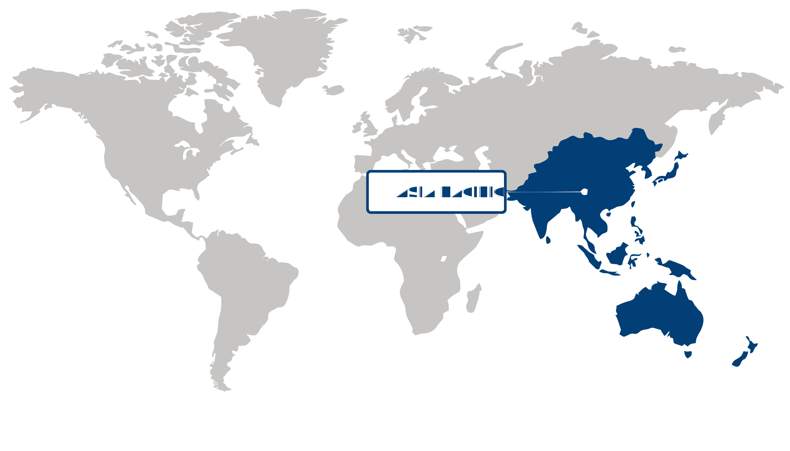
Holding the largest share of the photomask repair system market, Asia Pacific led the regional landscape in 2026, supported by its strong semiconductor manufacturing ecosystem and concentration of advanced electronics production. Photomask repair systems are essential for maintaining mask quality and reducing defects during semiconductor fabrication, making demand closely tied to the expansion and technological advancement of chip manufacturing facilities. The region's extensive semiconductor supply chain, growing investment in fabrication capabilities, and increasing need for high-precision manufacturing processes reinforce adoption of sophisticated repair technologies. Continued advancement in semiconductor designs and tighter manufacturing requirements further strengthen the strategic importance of photomask inspection and repair capabilities.
Europe (Fastest-Growing Region)
Europe is the fastest-growing region, supported by increasing investment in semiconductor technologies, advanced electronics manufacturing, and efforts to strengthen regional supply-chain resilience. The expansion of specialized fabrication and research capabilities is creating greater demand for precision equipment that can improve manufacturing yield and maintain stringent mask quality requirements. Europe's established engineering expertise and growing focus on technologically advanced semiconductor applications provide a foundation for photomask repair system adoption. Furthermore, increased attention to domestic semiconductor capabilities and advanced manufacturing infrastructure is encouraging investment in equipment that supports reliable and efficient fabrication processes.
| Parameter | North America | Asia Pacific | Europe | Latin America | MEA |
|---|---|---|---|---|---|
| Innovation Hub i Scale Nascent Developing Advanced | |||||
| Cost-Sensitive Region i Scale Low Medium High | |||||
| Regulatory Environment i Scale Restrictive Neutral Supportive | |||||
| Demand Drivers i Scale Weak Moderate Strong | |||||
| Development Stage i Scale Emerging Developing Developed | |||||
| Adoption Rate i Scale Low Medium High | |||||
| New Entrants / Startups i Scale Sparse Moderate Dense | |||||
| Macro Indicators i Scale Weak Stable Strong |
Key Country Insights
Germany 🇩🇪
Precision Inspection CapabilityGermany advances photomask repair system adoption through semiconductor manufacturing and precision engineering expertise. Companies prioritize high-resolution repair technologies that improve fabrication quality while supporting increasingly complex integrated circuit designs.
France 🇫🇷
Microelectronics Quality SupportFrance strengthens photomask repair capabilities through research-intensive microelectronics activities and specialized semiconductor production. Organizations prioritize systems that deliver accurate repairs while supporting advanced manufacturing and technology development initiatives.
Italy 🇮🇹
Specialized Semiconductor InfrastructureItaly applies photomask repair systems within specialized semiconductor manufacturing and research environments focused on precision production. Equipment selection increasingly favors flexible platforms capable of supporting diverse fabrication requirements and evolving process technologies.
Japan 🇯🇵
Lithography Process EnhancementJapan maintains strong demand for photomask repair systems as semiconductor manufacturers pursue tighter process control and defect reduction. Local technology providers emphasize repair precision, equipment reliability, and compatibility with advanced lithography workflows.
South Korea 🇰🇷
Advanced Chip FabricationSouth Korea relies on photomask repair systems to support high-volume semiconductor production and advanced memory manufacturing. Investments center on rapid defect identification and repair capabilities that help maintain fabrication efficiency and product quality.
United States 🇺🇸
Semiconductor Yield OptimizationThe U.S. photomask repair system market is supported by semiconductor fabrication and advanced chip design activities requiring precise defect correction. Equipment suppliers focus on automation, inspection accuracy, and integration with modern lithography production environments.
Segment Leadership and Growth Trends
Photomask Repair System Market Share (%), by Application, 2026
Go beyond the chart, access full insights & data tables
Request Free Sample ReportApplication Segment Analysis: Mask Shops (Largest Segment) vs Semiconductor Device Manufacturers (Fastest-Growing Segment)
Mask shops dominated the photomask repair system market in 2026, accounting for a 71.04% share, as they routinely handle photomask inspection, defect correction, and refurbishment across a broad range of semiconductor and display manufacturing requirements. The increasing complexity of mask patterns and the need to maintain high-quality masks throughout repeated production cycles make reliable repair capabilities essential. Repair systems help mask shops extend mask usability, reduce replacement requirements, and maintain stringent pattern accuracy, supporting their strong position in the application landscape.
Semiconductor device manufacturers represent the fastest-growing application as advanced semiconductor fabrication increasingly depends on highly precise photomasks and tighter defect-control requirements. Bringing repair capabilities closer to manufacturing operations can support faster defect resolution, improve process responsiveness, and reduce disruptions associated with sending masks to external facilities. The continued evolution toward more intricate device structures is also increasing the importance of accurate, localized repair technologies.
Type Segment Analysis: Nanomachining Technology (Largest Segment) vs Laser Technology (Fastest-Growing Segment)
Nanomachining technology held the largest share of the photomask repair system market in 2026, reflecting its ability to perform highly controlled material removal and precise defect correction on complex mask structures. The technology is well suited to applications where dimensional accuracy and surface quality are critical, particularly as photomask designs become increasingly sophisticated. Its established role in precision repair workflows and compatibility with demanding defect-correction requirements supports continued adoption.
Laser technology is advancing rapidly because it offers contactless and highly localized material processing, enabling efficient correction of selected mask defects while minimizing mechanical interaction with delicate surfaces. Improvements in beam control, process precision, and automation are enhancing its suitability for increasingly demanding photomask repair tasks. Growing interest in faster and more flexible repair processes is encouraging greater adoption of laser-based systems.
| Segment | Sub-Segment | Largest Segment | Fastest Growing |
|---|---|---|---|
| Application | Semiconductor Device Manufacturers, Mask Shops | Mask Shops | Semiconductor Device Manufacturers |
| Type | Laser Technology, Focused Ion Beam (FIB)Technology, Nanomachining Technology | Nanomachining Technology | Laser Technology |
Competitive Landscape and Market Positioning
Leading companies in the photomask repair system market:
1. Carl Zeiss AG (Germany)
2. KLA Corporation (United States)
3. Lasertec Corporation (Japan)
4. Hitachi High-Tech Corporation (Japan)
5. JEOL Ltd. (Japan)
6. Park Systems Corp. (South Korea)
7. DAEIL SYSTEMS Co. Ltd. (South Korea)
8. COWIN DST Co. Ltd. (South Korea)
9. Bruker Corporation (United States)
10. Hamamatsu Photonics K.K. (Japan)
The photomask repair system market is advancing with improved precision repair technologies supporting semiconductor manufacturing needs. Innovation in defect detection and correction methods is enhancing yield efficiency. New system developments are enabling faster and more accurate repair processes. The photomask repair system market continues to evolve with increasing demand for high-precision semiconductor fabrication tools.
| Company | Market Share | Company Revenue | Revenue CAGR (%) | Product Portfolio | Geographic Presence | Innovation / R&D Focus | Strategic Developments |
|---|---|---|---|---|---|---|---|
| Carl Zeiss AG (Germany) | |||||||
| KLA Corporation (United States) | |||||||
| Lasertec Corporation (Japan) | |||||||
| Hitachi High-Tech Corporation (Japan) | |||||||
| JEOL Ltd. (Japan) | |||||||
| Park Systems Corp. (South Korea) | |||||||
| DAEIL SYSTEMS Co. Ltd. (South Korea) | |||||||
| COWIN DST Co. Ltd. (South Korea) | |||||||
| Bruker Corporation (United States) | |||||||
| Hamamatsu Photonics K.K. (Japan). |
Industry Development/News
| Company Name | Date | Key Development |
|---|
Customize Your Report
Explore examples of how this report can be tailored to different research needs, including custom segments, additional topics or chapters, and related reports. Click a section of the wheel or its numbered marker to explore the available options.
Photomask Repair System Market — Custom Segments
| Segment | Sub-Segment |
|---|---|
| Defect Type | Particle Defects, Pattern Defects, Pinholes & Voids, Scratches & Surface Defects |
| Photomask Type | Binary Masks, Phase-Shift Masks, EUV Masks, Optical Blank Masks |
| Semiconductor Technology Node | Mature Nodes, 28–65 nm, 7–16 nm, Below 7 nm |
Photomask Repair System Market — Custom TOC
| Custom Chapter | Custom Details |
|---|---|
| Semiconductor Yield Enhancement Strategies |
|
| Advanced Photomask Technology Roadmap |
|
| Next-Generation Lithography Impact Assessment |
|
Need a different cut of the data?
Request Custom ResearchWhat is the market size of photomask repair system?
How is the photomask repair system industry expected to grow over the next 10 years?
Why are advanced semiconductor nodes increasing investment in photomask repair systems?
How is semiconductor miniaturization influencing purchasing priorities in the photomask repair system market?
Why do mask shops dominate the photomask repair system market?
Why is laser technology the fastest-growing type in the photomask repair system market?
What makes Asia Pacific the largest photomask repair system market?
What is driving photomask repair system market growth in Europe?
Which organizations are considered leaders in the photomask repair system landscape?
Our Clients
"Working with FBI has been a good experience. The market report provided a holistic view, covering everything from emerging trends to potential risks."
Semtech Corporation
"The experience was highly positive. The team showcased remarkable flexibility in adapting to our specific needs and delivered report that perfectly aligned with all our requirements."
TSMC
"What really stood out to me was how clearly and promptly the Fundamental Business Insights team communicated throughout. It made the collaboration feel effortless."
NXP Semiconductors
Our Research Team & Methodology
Every Fundamental Business Insights report is built by a dedicated vertical research team, validated through a structured primary-and-secondary methodology, and reviewed for accuracy before it reaches you.
Research Team Overview
Prepared by the Electronics & Semiconductors Research Team
Delivery
Published
Demand
Available
Support
Trust & Compliance
Research Domains
10 coverage areasResearch Intelligence
| Source | Reference |
|---|---|
| Semiconductor Industry Association (SIA) | www.semiconductors.org |
| SEMI | www.semi.org |
| JEDEC Solid State Technology Association | www.jedec.org |
| IEEE | www.ieee.org |
| IPC – Association Connecting Electronics Industries | www.ipc.org |
| International Electrotechnical Commission (IEC) | www.iec.ch |
| International Organization for Standardization (ISO) | www.iso.org |
| U.S. Bureau of Industry and Security (BIS) | www.bis.gov |
| U.S. Patent and Trademark Office (USPTO) | www.uspto.gov |
| European Patent Office (EPO) | www.epo.org |
| Taiwan Semiconductor Industry Association (TSIA) | www.tsia.org.tw |
| World Semiconductor Trade Statistics (WSTS) | www.wsts.org |
| International Energy Agency (IEA) | www.iea.org |
| GSMA | www.gsma.com |
| 3GPP | www.3gpp.org |
| ITU (International Telecommunication Union) | www.itu.int |
| Omdia (public insights) | omdia.tech.informa.com |
| Display Supply Chain Consultants (DSCC) | www.displaysupplychain.com |
| U.S. Department of Energy (DOE) | www.energy.gov |
| NIST (National Institute of Standards and Technology) | www.nist.gov |
Research Workflow & Quality Assurance
Data Collection
Verified information gathered through primary and secondary research.
Data Triangulation
Cross-validation using multiple independent data sources.
Forecast Modelling
Market estimates developed using historical trends and analytical models.
Analyst Validation
Findings reviewed by domain experts for accuracy and consistency.
Editorial & Quality Review
Final editorial, quality, and compliance checks before publication.
Final Publication
Released after successful completion of the internal review process.
Report Coverage
📊 Market Assessment
- Market Size & Forecast
- Market Segmentation
- Regional Analysis
- Growth Drivers & Challenges
- Market Dynamics
🏢 Competitive Intelligence
- Competitive Landscape
- Company Profiles
- Competitive Benchmarking
- Mergers & Acquisitions
- Market Share Analysis or Key Company Strategies
🔍 Strategic Analysis
- Value Chain Analysis
- Porter's Five Forces
- PESTLE Analysis
- Pricing Trends
- Supply-Demand Analysis
🚀 Future Outlook
- Technology Landscape
- Regulatory Landscape
- Investment & Funding Landscape
- Emerging Opportunities
- Future Market Outlook
Have a question about this report or need a custom scope?
Request Customization