Focused Ion Beam Market Size & Forecasts 2026-2035, By Segments (Ion Source, Application), Growth Opportunities, Innovation Landscape, Regulatory Shifts, Strategic Regional Insights (U.S., Japan, China, South Korea, UK, Germany, France), and Competitive Dynamics (Thermo Fisher Scientific, Hitachi High-Technologies, JEOL, Raith, TESCAN)
Market Size and Growth Outlook
Focused Ion Beam Market size is expected to advance from USD 1.52 billion in 2025 to USD 3.1 billion by 2035, registering a CAGR of more than 7.4% across 2026-2035. By 2026, the industry is anticipated to generate USD 1.62 billion in revenue.
Get more details on this report
Request Free Sample ReportFocused Ion Beam Market Intelligence Snapshot
Regional Market Dynamics
Segment Momentum
Market Expansion Drivers
Leading Market Participants
Global Market Forecast Snapshot
Market Outlook
Regional and Segment Outlook
Market Growth Drivers and Industry Trends
Expansion in Advanced Electronics and MEMS Fabrication: Growth of sensors, advanced packaging and MEMS for automotive and consumer electronics is increasing prototyping and rework demands that feed the focused ion beam market. Bosch and STMicroelectronics scaling MEMS production and Applied Materials’ work on packaging demonstrate industry-side needs for rapid failure analysis and precision machining. Large vendors can bundle FIB with packaging and test solutions, whereas new entrants and service labs can capture early-stage prototyping and short-run MEMS repair opportunities; ongoing manufacturing announcements and supply-chain adjustments suggest persistent, equipment-driven uptake.
Emerging Applications in Nanotechnology and Biomedical Devices: Uptake of FIB in nanofabrication and biological sample preparation is broadening end‑user bases for the focused ion beam market. Thermo Fisher Scientific’s cryo‑FIB solutions for cryo‑EM and published work from Harvard University and Johns Hopkins University using FIB for nanoscale device fabrication and tissue sample prep underscore cross-disciplinary demand. Incumbents can expand into correlative workflows and regulated life‑science channels, while startups and contract research organizations can specialize in application-specific process recipes; the visible commercialization of cryo‑FIB tools and academic adoption points to durable diversification into bio‑nanotech applications.
Industry Restraints:
High Capital and Operating Costs
Focused ion beam (FIB) systems require outsized upfront and lifecycle investment—advanced platforms such as Thermo Fisher Scientific’s Helios and Carl Zeiss’s Crossbeam series demand cleanroom integration, vibration isolation, and specialized maintenance—so purchasers face not only purchase price but recurring costs for ion sources, vacuum pumps and service from vendors like Oxford Instruments. SEMI’s equipment reporting underscores high capital intensity across microelectronics tool categories, which depresses adoption among smaller failure‑analysis labs and forces longer replacement cycles at tier‑2 customers. Strategically, incumbents benefit from aftermarket service revenues while new entrants face steep barriers to scale and financing; consortium buys and tool‑sharing models emerge as mitigants. Expect cost sensitivity to persist near term, driving modular tool designs, rental/servicing models, and consolidation among service providers.
Export Controls and Dual‑Use Regulations
Controls on advanced semiconductor and analysis equipment constrain addressable markets and customer engagement: the U.S. Department of Commerce Bureau of Industry and Security (BIS) and multilateral frameworks such as the Wassenaar Arrangement have tightened rules that affect shipment of precision ion‑beam and imaging systems, a dynamic highlighted by export challenges faced by major equipment suppliers including ASML in adjacent lithography segments. Compliance adds licensing delays, restricts sales to certain geographies and raises legal and audit costs for vendors and purchasers. For market participants, established firms must invest in global compliance teams while challengers may find market access fragmented; channel strategies and local partnerships become essential. Geopolitical scrutiny is likely to remain a gating factor in the near to medium term, shaping customer targeting and supply‑chain localisation strategies.
| Growth Driver | Impact on CAGR | Regulatory Influence | Geographic Relevance | Adoption Rate | Impact Timeline |
|---|---|---|---|---|---|
| Increasing adoption in semiconductor and materials research | 2.00% | Short term (≤ 2 yrs) | North America, Asia Pacific | Medium | Fast |
| Expansion in advanced electronics and MEMS fabrication | 1.80% | Medium term (2–5 yrs) | Asia Pacific, Europe | Medium | Moderate |
| Emerging applications in nanotechnology and biomedical devices | 1.20% | Long term (5+ yrs) | North America, Europe | Low | Moderate |
Unlock insights tailored to your business with our bespoke market research solutions.
Click to get your customized report now.
Regional Demand Dynamics
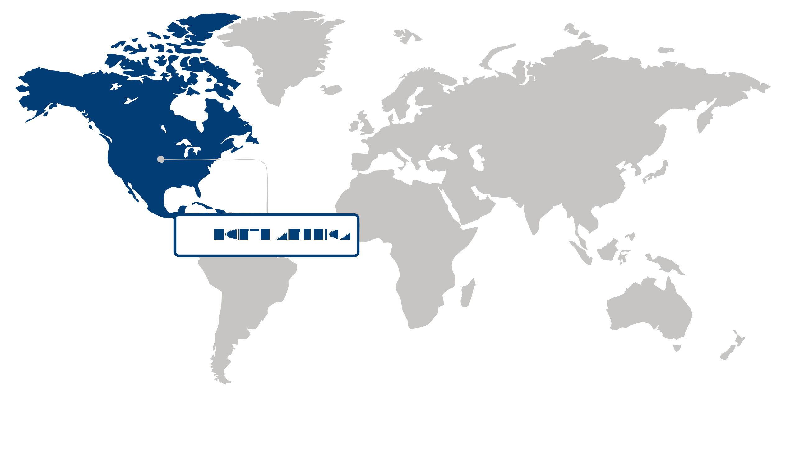
North America captured over 34.7% of the focused ion beam market in 2025, remaining the largest regional share. This leadership is rooted in concentrated semiconductor manufacturing and high R&D intensity—underscored by the U.S. CHIPS and Science Act and regular commentary from the Semiconductor Industry Association that have spurred onshore capacity expansions. Strong public research ecosystems, exemplified by Lawrence Berkeley National Laboratory and National Science Foundation-supported university programs, and equipment suppliers such as Thermo Fisher Scientific and Applied Materials reporting elevated demand, reinforce adoption. Supply-chain reshoring, skilled talent pools, and regulatory support for advanced manufacturing further accelerate uptake. Given continued public-private investment and the presence of flagship fabs and labs, North America offers sustained opportunities across instruments, process integration, and specialized services.
The United States anchors the North American market, concentrating fabs, national labs, and corporate R&D that drive demand for focused ion beam market capabilities. U.S. Department of Commerce implementation of the CHIPS Act and Intel and TSMC announcements for new U.S. facilities illustrate equipment and metrology pull; Sandia National Laboratories and Lawrence Livermore National Laboratory provide high-end science use cases. Thermo Fisher Scientific and Applied Materials customer engagements and National Science Foundation funding streams create a pipeline for advanced FIB deployments. Strategically, vendors and investors should prioritize high-throughput, application-specific tools and service partnerships to capture lab-to-fab and defense-related demand across the region.
Asia Pacific Market Analysis:
Asia Pacific emerged as the fastest-growing region in the focused ion beam market, registering a robust CAGR of 10.1% as rapid expansion of semiconductor fabrication capacity, rising nanofabrication demand, and increasing research investments accelerate tool demand. Major wafer manufacturers’ capacity announcements — notably TSMC and Samsung Electronics — and China’s National Integrated Circuit Industry Investment Fund have driven demand for advanced failure analysis and mask repair capabilities supplied by JEOL, Hitachi High‑Tech and Thermo Fisher Scientific. Government incentives from Japan’s Ministry of Economy, Trade and Industry and research funding from institutions such as the Chinese Academy of Sciences and RIKEN are aligning capital and talent around nanoscale process control. This combination of production scale-ups, equipment sourcing strategies and concentrated R&D investment makes APAC a high-opportunity region for focused ion beam vendors and service providers.
China serves as a central manufacturing and scale-play within the focused ion beam market, where state-directed capital and domestic foundry growth shape procurement and deployment. The National Integrated Circuit Industry Investment Fund has backed capacity and domestic supply-chain development, and SMIC’s announced capacity projects and local research hubs at the Chinese Academy of Sciences have expanded in-house failure-analysis needs, increasing demand for site-specific milling and cross-sectioning. Domestic purchasing patterns favor instrument suppliers that can offer local service and integration with wafer fabs, while academic hubs push higher-resolution applications. For vendors, tailoring service models, training and spare-parts logistics to China’s large foundry and research base is a direct route to capture regional volume and advanced-use cases.
Japan plays a specialized, high-value role in the focused ion beam market, driven by its strength in precision equipment manufacturing and advanced research collaborations. JEOL and Hitachi High‑Tech supply precision FIB and FIB‑SEM systems to domestic fabs and research institutes, while METI’s incentive programs and corporate R&D at organizations like RIKEN and the University of Tokyo sustain demand for nanofabrication and failure-analysis capabilities. Japanese procurement emphasizes uptime, precision and integration with electron microscopy workflows, favoring suppliers with strong service networks and instrument reliability. Japan’s combination of equipment expertise, government support and concentrated research creates a strategic hub that complements broader APAC volume growth and accelerates adoption of higher-specification focused ion beam applications.
Europe Market Trends:
Europe held a substantial share of the focused ion beam market, reflecting a dense concentration of research centers, advanced manufacturing and targeted policy support that sustain equipment demand and services. Demand is reinforced by the European Commission’s Chips Act and Horizon Europe funding alongside project financing from the European Investment Bank, while tool and service supply is anchored by Thermo Fisher Scientific, Carl Zeiss Microscopy and Raith GmbH and by research users such as Fraunhofer-Gesellschaft, CEA-Leti and CERN. Operationally, strong engineering talent, cross-border supply-chain consolidation and sustainability-driven process optimization are evident. These factors position Europe for continued commercialization of advanced FIB applications across semiconductors, materials science and failure analysis, creating sizable entry and partnership opportunities.
Germany functions as a manufacturing and application hub in the focused ion beam market, driven by large-scale demand from automotive and power-semiconductor players. Homegrown customers and collaborators such as Infineon Technologies AG, Robert Bosch GmbH and Fraunhofer institutes accelerate adoption of FIB for device qualification and packaging, while the Federal Ministry for Economic Affairs and Climate Action supports industrial modernization. Strong OEM-supplier relationships, localized pilot lines and skilled technical workforce make Germany a priority market for equipment vendors and service providers seeking high-volume, high-value engagements that scale regionally.
France occupies a strategic R&D and innovation role in the focused ion beam market, anchored by national research and industrialization engines. Institutions such as CEA-Leti, CNRS and STMicroelectronics, together with financing and industrialization programs under France 2030 and Bpifrance, drive early-stage process development, prototype scaling and start-up formation. This innovation pipeline creates demand for specialized FIB tools and contract services, offering suppliers opportunities to partner on commercialization pathways and to leverage French-led projects to access broader European research and manufacturing networks.
| Parameter | North America | Asia Pacific | Europe | Latin America | MEA |
|---|---|---|---|---|---|
| Innovation Hub i Scale Nascent Developing Advanced | |||||
| Cost-Sensitive Region i Scale Low Medium High | |||||
| Regulatory Environment i Scale Restrictive Neutral Supportive | |||||
| Demand Drivers i Scale Weak Moderate Strong | |||||
| Development Stage i Scale Emerging Developing Developed | |||||
| Adoption Rate i Scale Low Medium High | |||||
| New Entrants / Startups i Scale Sparse Moderate Dense | |||||
| Macro Indicators i Scale Weak Stable Strong |
Segment Leadership and Growth Trends
Focused Ion Beam Market Share (%), by Ion Source, 2026
Go beyond the chart, access full insights & data tables
Request Free Sample ReportGallium held largest share in 2025 in the focused ion beam market for the Ion Source segment, reflecting its widespread use in nanofabrication and semiconductor failure analysis. Its dominance is underpinned by compatibility with leading platforms from Thermo Fisher Scientific and JEOL Ltd., predictable milling behavior valued by customers, and established service and supply networks that reduce process variability. Thermo Fisher Scientific application notes and JEOL Ltd. case studies document Ga-based workflows for TEM sample prep and circuit edit, reinforcing adoption. This creates strategic openings for incumbents to bundle hardware, software, and support, while challengers can target niche segments with alternative ion chemistries or software-enabled precision; reliance on Ga-driven workflows and industry validation points to continued near-term relevance.
Analysis by Application
Nanofabrication represented largest share in 2025 in the focused ion beam market for the Application segment, driven by demand for high-precision patterning in semiconductors, MEMS, and academic research. Industry adoption is evident in use cases reported by Intel and IBM Research and in NIST methodologies that employ FIB for device prototyping and metrology, reflecting customer preference for deterministic, high-resolution processing. Supply-chain integration, digital process controls, and tighter regulatory standards for advanced nodes favor turnkey solutions, offering established vendors scale advantages and newcomers opportunities in AI-enabled process control or specialized service offerings; continued device miniaturization and MEMS growth support sustained relevance.
| Segment | Sub-Segment | Largest Segment | Fastest Growing |
|---|---|---|---|
| Ion Source | Gallium, Iridium, Gold, Others | ||
| Application | Nanofabrication, Failure Analysis, Material Science, Device Modification, Sample Preparation, Circuit Edit, Others |
Competitive Landscape and Market Positioning
Competitive dynamics are driven by portfolio integration, capability accretion, and closer alignment with fabs and research centers. Leading suppliers have expanded instrument suites and tightened technical links with high‑value end users while accelerating software, automation, and advanced ion‑source developments. These moves favor turnkey, application‑specific solutions and stronger service ecosystems, prompt smaller vendors to pursue specialization, and shift competition toward reproducible workflows, user experience, and cross‑technology interoperability.
Strategic / Actionable Recommendations for Regional Players
North America: Leverage dense fabrication and national‑lab ecosystems by deepening technical partnerships, prioritizing automation and field service excellence, and tailoring offerings to advanced packaging, failure analysis, and high‑throughput R&D users.
Asia Pacific: Expand local production and channel collaborations to address cost sensitivity, co‑develop instruments with regional OEMs and research centers, and focus on wafer‑level, memory, and high‑volume test workflows.
Europe: Concentrate on high‑precision, customizable systems for materials science and large research infrastructures, strengthen ties with universities and funding consortia, and position as providers of compliance‑aware, turnkey solutions for specialized industrial users.
| Company | Market Share | Company Revenue | Revenue CAGR (%) | Product Portfolio | Geographic Presence | Innovation / R&D Focus | Strategic Developments |
|---|---|---|---|---|---|---|---|
| No companies available. | |||||||
Industry Development/News
| Company Name | Date | Key Development |
|---|
Customize Your Report
Explore examples of how this report can be tailored to different research needs, including custom segments, additional topics or chapters, and related reports. Click a section of the wheel or its numbered marker to explore the available options.
Focused Ion Beam Market — Custom Segments
| Segment | Sub-Segment |
|---|---|
| No segment data available. | |
Focused Ion Beam Market — Custom TOC
| Custom Chapter | Custom Details | ||
|---|---|---|---|
| No custom TOC data available. | |||
Need a different cut of the data?
Request Custom ResearchWhat is the current revenue of the focused ion beam market?
What is the projected value of the focused ion beam industry by 2035?
In which region is the focused ion beam market most concentrated?
Which region shows the most rapid acceleration in the focused ion beam sector?
Why does gallium sub-segment dominate the ion source segment of focused ion beam sector?
How does nanofabrication segment fare in the focused ion beam industry?
Which companies are driving growth in the focused ion beam landscape?
Our Clients
"Working with FBI has been a good experience. The market report provided a holistic view, covering everything from emerging trends to potential risks."
Semtech Corporation
"The experience was highly positive. The team showcased remarkable flexibility in adapting to our specific needs and delivered report that perfectly aligned with all our requirements."
TSMC
"What really stood out to me was how clearly and promptly the Fundamental Business Insights team communicated throughout. It made the collaboration feel effortless."
NXP Semiconductors
Our Research Team & Methodology
Every Fundamental Business Insights report is built by a dedicated vertical research team, validated through a structured primary-and-secondary methodology, and reviewed for accuracy before it reaches you.
Research Team Overview
Prepared by the Electronics & Semiconductors Research Team
Delivery
Published
Demand
Available
Support
Trust & Compliance
Research Domains
10 coverage areasResearch Intelligence
| Source | Reference |
|---|---|
| Semiconductor Industry Association (SIA) | www.semiconductors.org |
| SEMI | www.semi.org |
| JEDEC Solid State Technology Association | www.jedec.org |
| IEEE | www.ieee.org |
| IPC – Association Connecting Electronics Industries | www.ipc.org |
| International Electrotechnical Commission (IEC) | www.iec.ch |
| International Organization for Standardization (ISO) | www.iso.org |
| U.S. Bureau of Industry and Security (BIS) | www.bis.gov |
| U.S. Patent and Trademark Office (USPTO) | www.uspto.gov |
| European Patent Office (EPO) | www.epo.org |
| Taiwan Semiconductor Industry Association (TSIA) | www.tsia.org.tw |
| World Semiconductor Trade Statistics (WSTS) | www.wsts.org |
| International Energy Agency (IEA) | www.iea.org |
| GSMA | www.gsma.com |
| 3GPP | www.3gpp.org |
| ITU (International Telecommunication Union) | www.itu.int |
| Omdia (public insights) | omdia.tech.informa.com |
| Display Supply Chain Consultants (DSCC) | www.displaysupplychain.com |
| U.S. Department of Energy (DOE) | www.energy.gov |
| NIST (National Institute of Standards and Technology) | www.nist.gov |
Research Workflow & Quality Assurance
Data Collection
Verified information gathered through primary and secondary research.
Data Triangulation
Cross-validation using multiple independent data sources.
Forecast Modelling
Market estimates developed using historical trends and analytical models.
Analyst Validation
Findings reviewed by domain experts for accuracy and consistency.
Editorial & Quality Review
Final editorial, quality, and compliance checks before publication.
Final Publication
Released after successful completion of the internal review process.
Report Coverage
📊 Market Assessment
- Market Size & Forecast
- Market Segmentation
- Regional Analysis
- Growth Drivers & Challenges
- Market Dynamics
🏢 Competitive Intelligence
- Competitive Landscape
- Company Profiles
- Competitive Benchmarking
- Mergers & Acquisitions
- Market Share Analysis or Key Company Strategies
🔍 Strategic Analysis
- Value Chain Analysis
- Porter's Five Forces
- PESTLE Analysis
- Pricing Trends
- Supply-Demand Analysis
🚀 Future Outlook
- Technology Landscape
- Regulatory Landscape
- Investment & Funding Landscape
- Emerging Opportunities
- Future Market Outlook
Have a question about this report or need a custom scope?
Request Customization