Flip Chip Bonder Market Size & Forecasts 2026-2035, By Segments (Type, Application, End-User), Growth Opportunities, Innovation Landscape, Regulatory Shifts, Strategic Regional Insights (U.S., Japan, China, South Korea, UK, Germany, France), and Competitive Dynamics (ASM Pacific, Kulicke & Soffa, Samsung Electronics, K&S, MRSI Systems)
Market Size and Growth Outlook
Flip Chip Bonder Market size is forecasted to reach USD 429.58 million by 2035, rising from USD 304.54 million in 2025, at a CAGR of more than 3.5% between 2026 and 2035. In 2026, revenue is projected at USD 313.59 million.
Get more details on this report
Request Free Sample ReportFlip Chip Bonder Market Intelligence Snapshot
Regional Market Dynamics
Segment Momentum
Market Expansion Drivers
Leading Market Participants
Global Market Forecast Snapshot
Market Outlook
Regional and Segment Outlook
Market Growth Drivers and Industry Trends
Expansion of outsourced semiconductor assembly and packaging (OSAT) capacity and OEM moves toward heterogeneous integration are raising demand for high-throughput flip-chip tooling, as evidenced by SEMI commentary and Amkor Technology capacity expansion announcements that align with factory modernization initiatives. These changes affect the flip chip bonder market by concentrating capital expenditure on equipment that supports finer-pitch and higher-density assemblies, creating opportunities for incumbents to offer integrated bonding-plus-automation systems and for new entrants to serve regional OSATs with flexible, lower-capex solutions. Given publicly announced OSAT investments and SEMI roadmaps, equipment demand will follow continued packaging complexity in the near term.
Increasing adoption of flip-chip technology in consumer electronics
Wider use of flip-chip interconnects in smartphones, wearables and AR/VR modules—driven by design choices from TSMC, Apple and Samsung Electronics—raises precision and throughput requirements that directly shape the flip chip bonder market. TSMC’s InFO/CoWoS product roadmaps and Samsung’s packaging work for image sensors (including collaborations with Sony) demonstrate OEM-driven shifts that favor advanced bonders with inline inspection. Established vendors can scale to meet high-volume needs while startups can differentiate on AI-enabled process control and compact systems for niche device makers. Observable product roadmaps from major foundries indicate steady integration of flip-chip architectures into consumer roadmaps.
Development of advanced bonding materials and adhesives
New underfills, conductive adhesives and low-temperature solders from Henkel and Indium Corporation, alongside material research at IMEC, are enabling finer-pitch, higher-reliability bonds and altering process parameters that equipment must support, as reflected in supplier technical literature and IMEC publications. These material advances affect the flip chip bonder market by requiring machines with tighter thermal and dispensing control; partnerships between equipment OEMs and material suppliers present win-win opportunities, while entrants can specialize in material-integrated tooling or analytics. With material qualification cycles accelerating at research centers like IMEC and sustainability guidance from the European Chemicals Agency, bonders will increasingly need adaptable platforms to accommodate new chemistries.
Industry Restraints:
Supply Chain Vulnerabilities for Advanced Packaging Materials
Chronic shortages and long lead times for critical inputs—underfill adhesives, copper-pillar bumps, high-density interposers and specialized flux—constrain throughput and raise unit costs, reducing OEM willingness to expand flip chip capacity. SEMI has documented extended equipment and materials lead times across advanced packaging supply chains, and Henkel has highlighted surging demand for underfill solutions in its corporate communications, while ASE Technology Holding has publicly announced capacity expansions driven by tight packaging supply. For incumbents this forces prioritization of high-margin customers and vertical integration; for new entrants it raises barriers to entry and working-capital requirements. Absent rapid upstream capacity additions and supplier diversification, these supply constraints will likely continue to dictate production pacing and pricing dynamics in the near to medium term.
High Capital Intensity and Equipment Complexity
Deploying state-of-the-art flip chip bonders requires substantial capital expenditure, specialized metrology, and sustained R&D to maintain yield and cycle time advantages, slowing adoption among smaller assemblers. Kulicke & Soffa and ASM Pacific Technology have emphasized in investor presentations the heavy investment and continuous equipment upgrades needed for advanced die-attach and underfill processes, and U.S. Department of Commerce CHIPS-era funding signals recognition that public support is necessary to offset private capital barriers. For market leaders, this favors scale players that can amortize equipment and innovation costs; for challengers, securing funding and proving process stability are major hurdles. Expect continued consolidation and selective public-private investment to shape competitive positioning over the coming years.
| Growth Driver | Impact on CAGR | Regulatory Influence | Geographic Relevance | Adoption Rate | Impact Timeline |
|---|---|---|---|---|---|
| Growth in semiconductor assembly and packaging | 1.50% | Short term (≤ 2 yrs) | Asia Pacific, North America | Medium | Fast |
| Increasing adoption of flip-chip technology in consumer electronics | 1.00% | Medium term (2–5 yrs) | North America, Asia Pacific | Low | Moderate |
| Development of advanced bonding materials and adhesives | 1.00% | Long term (5+ yrs) | Europe, Asia Pacific | Medium | Slow |
Unlock insights tailored to your business with our bespoke market research solutions.
Click to get your customized report now.
Regional Demand Dynamics
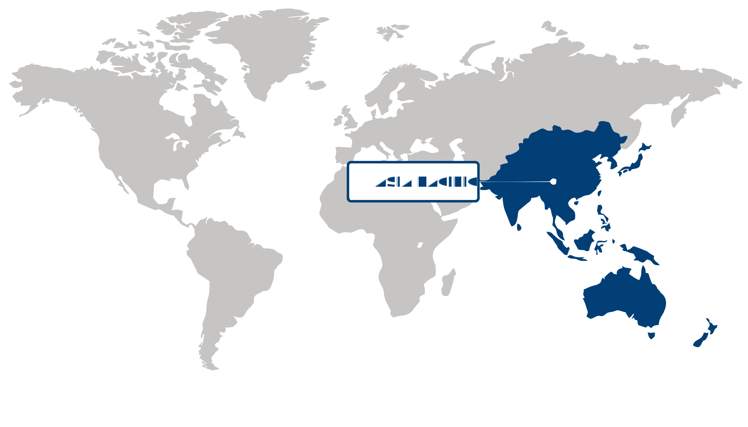
Asia Pacific captured approximately 60.00% of the global flip chip bonder market in 2025, remaining the largest regional base driven by massive semiconductor production and packaging hubs in Taiwan and South Korea; Taiwan Semiconductor Manufacturing Company (TSMC) and Samsung Electronics underpin sustained demand as they scale advanced packaging, while ASE Technology Holding and Amkor increase substrate and assembly throughput. Strong capital intensity, concentrated supplier networks, government incentives and close OEM-packager relationships continue to accelerate uptake of high-throughput bonders, and public filings from TSMC and Samsung Electronics alongside facility expansions by ASE illustrate tangible capacity-led demand. These factors position the region for continued strategic investment and technology adoption in flip chip assembly.
Japan is positioned as a pivotal hub in Asia Pacific for the flip chip bonder market, supplying precision equipment, materials and high-reliability components that complement neighboring packaging centers. Suppliers such as Tokyo Electron and Sumitomo Chemical, together with policy direction from the Ministry of Economy, Trade and Industry (METI), emphasize advanced process control and materials innovation that serve automotive and industrial customers requiring low-defect, high-reliability interconnects. Japan’s equipment leadership and specialized workforce create downstream opportunities for regional packagers and OEMs seeking quality-differentiated flip chip assembly.
China is emerging as a major demand center in Asia Pacific for the flip chip bonder market, where rising domestic system integration and government support expand local packaging capacity. Foundry and fab players such as Semiconductor Manufacturing International Corporation (SMIC) and large system vendors like Huawei, supported by initiatives from the Ministry of Industry and Information Technology (MIIT), are accelerating in-country assembly and test, increasing demand for automated bonders. China’s scale and policy-backed localization reinforce regional supply-chain depth and create high-volume adjacent markets for equipment suppliers targeting Asia Pacific growth.
Europe Market Analysis:
Europe emerged as the fastest-growing region in the flip chip bonder market, registering a CAGR of 5.2%, driven by rising semiconductor demand across automotive and healthcare sectors. Policy support from the European Commission via the European Chips Act and targeted IPCEI projects has unlocked funding and site selection momentum, while lead customers in mobility and medical imaging are accelerating adoption; Infineon Technologies and Robert Bosch GmbH have publicly signaled capacity and packaging investments in Germany, and Siemens Healthineers’ device roadmaps are increasing advanced-packaging requirements. These dynamics, alongside localized talent pools and reshored supply-chain initiatives, position Europe to capture higher-value packaging work and specialist system-in-package flows over the next investment cycle. Europe therefore offers strategically concentrated opportunities for equipment suppliers and integrators.
Germany anchors the region’s manufacturing backbone in the flip chip bonder market, where automotive electrification and ADAS sensor scaling bite most sharply. Domestic demand patterns and supplier strategies—evident in statements from Infineon Technologies and Robert Bosch GmbH about capacity and packaging investments—have raised demand for high-throughput binders and fine-pitch alignment; incentive alignment under the European Chips Act and local cluster support accelerates capital deployment. For equipment vendors, Germany’s deep OEM-supplier ecosystems mean faster validation cycles and premium service opportunities, reinforcing regional momentum.
France plays a specialized role in the flip chip bonder market by concentrating on advanced packaging R&D and healthcare/industrial sensor applications. National initiatives such as France 2030 and collaborative programs at CEA-Leti, together with STMicroelectronics’ packaging capabilities in French sites, are channeling funding and pilot production toward system-in-package and medical-grade assemblies. This creates an innovation-rich environment for pilot lines and co-development with instrument OEMs, offering targeted entry points for bonders focused on precision, yield, and regulatory-ready workflows that complement Germany’s volume-driven demand.
North America Market Trends:
Held a substantial share, North America’s position in the flip chip bonder market is anchored by concentrated advanced-package demand and targeted policy support. Momentum reflects CHIPS and Science Act funding administered by the U.S. Department of Commerce, corporate investments such as Intel’s public statements on expanded packaging capacity, and supplier activity from equipment firms like Kulicke & Soffa, which cite North American backlog in press releases. Regional logistics and skilled labor pools in semiconductor clusters have enabled faster adoption of high-density interconnects and thermal-management processes, cited by the Semiconductor Industry Association. These factors position North America to capture premium bonders demand as enterprises and federal programs prioritize domestic advanced packaging.
The U.S. serves as the primary hub in the flip chip bonder market, propelled by hyperscale computing, automotive electrification, and defense procurement that require advanced packaging. Demand dynamics are evident in NVIDIA product roadmaps and Intel press releases pointing to higher-package complexity, while SkyWater Technology and Applied Materials communications highlight expanding domestic back-end services. Concurrent regulatory shifts from the Bureau of Industry and Security are reallocating some supply-chain activity onshore, increasing customer willingness to pay for localized assembly. Strategically, U.S. specialization in complex packages creates an anchor for North American suppliers and equipment makers to monetize premium bonder solutions and attract further investment.
| Parameter | North America | Asia Pacific | Europe | Latin America | MEA |
|---|---|---|---|---|---|
| Innovation Hub i Scale Nascent Developing Advanced | |||||
| Cost-Sensitive Region i Scale Low Medium High | |||||
| Regulatory Environment i Scale Restrictive Neutral Supportive | |||||
| Demand Drivers i Scale Weak Moderate Strong | |||||
| Development Stage i Scale Emerging Developing Developed | |||||
| Adoption Rate i Scale Low Medium High | |||||
| New Entrants / Startups i Scale Sparse Moderate Dense | |||||
| Macro Indicators i Scale Weak Stable Strong |
Segment Leadership and Growth Trends
Flip Chip Bonder Market Share (%), by Type, 2026
Go beyond the chart, access full insights & data tables
Request Free Sample ReportFully automatic dominated the flip chip bonder market in 2025 as the largest share among segments. Its leadership stems from rising adoption of high‑volume automated semiconductor assembly demanding speed and precision, a trend reinforced by SEMI equipment forecasts and TSMC and Intel press releases emphasizing automation and advanced packaging; supply‑chain consolidation, digitalized factories and skilled robotics teams further favor fully automatic lines. This segment creates strategic scale opportunities for established toolmakers and niche automation entrants, and will remain central near term as advanced-node packaging and throughput pressures sustain demand.
Analysis by Application
IDMs represented largest share in the flip chip bonder market in 2025 among segments. Growth is driven by integrated device manufacturers bringing packaging in‑house to control yield and timelines, evidenced by Intel’s IDM 2.0 announcements and Samsung Electronics’ packaging initiatives; this verticalization aligns with procurement resilience, IP protection and workforce upskilling trends. The shift opens partnerships for equipment suppliers and system integrators, and IDMs’ continued emphasis on end‑to‑end control suggests sustained relevance through the medium term.
Analysis by End-User
Consumer electronics held largest share in the flip chip bonder market in 2025 among segments. Leadership is propelled by booming demand for compact, high‑performance consumer devices that favor flip‑chip packaging, reflected in Apple and Samsung Electronics product strategies prioritizing smaller, faster chips and wafer‑level solutions; changing consumer preferences, rapid product cycles and regulatory energy efficiency goals further boost uptake. This creates fast‑moving opportunities for OSATs and automation providers, and the segment should remain pivotal as 5G, wearables and AR/VR device roadmaps continue to require dense packaging.
| Segment | Sub-Segment | Largest Segment | Fastest Growing |
|---|---|---|---|
| Type | Fully Automatic, Semi-Automatic | ||
| Application | IDMs, OSAT | ||
| End-User | Consumer Electronics, Healthcare, Telecommunications, Automotive, Aerospace & Defense |
Competitive Landscape and Market Positioning
The competitive landscape is shaped by intensified ecosystem alignment, selective portfolio expansion, and concentrated technology renewal: firms have deepened ties with OSATs and fabs, broadened service and retrofit offerings, and refreshed platforms to accelerate alignment, throughput and inspection convergence. Increased emphasis on platform modularity, localized support footprints, and targeted R&D has pushed differentiation toward end‑to‑end integration and faster time‑to‑qualification, reshaping relative positioning and raising the bar for operational responsiveness and innovation.
Strategic / Actionable Recommendations for Regional Players
Pursue closer collaboration with system integrators, OSATs and large end users to co-develop pilot lines and turnkey testing paths; prioritize digital automation and rapid prototyping to capture defense, automotive and specialized compute demand while strengthening aftersales service and qualification support.
Leverage proximity to major foundries and assembly ecosystems to scale volume production partnerships, invest in throughput-optimizing platform upgrades and localized supply continuity, and embed process development with leading OSATs to accelerate adoption across high-volume packaging segments.
Target high-reliability and regulated verticals by offering precision customization, retrofit service packages and compliance-ready process validation; deepen relationships with automotive and industrial OEMs and emphasize energy-efficient, space-optimized platforms and certified quality systems.
| Company | Market Share | Company Revenue | Revenue CAGR (%) | Product Portfolio | Geographic Presence | Innovation / R&D Focus | Strategic Developments |
|---|---|---|---|---|---|---|---|
| No companies available. | |||||||
Industry Development/News
| Company Name | Date | Key Development |
|---|
Customize Your Report
Explore examples of how this report can be tailored to different research needs, including custom segments, additional topics or chapters, and related reports. Click a section of the wheel or its numbered marker to explore the available options.
Flip Chip Bonder Market — Custom Segments
| Segment | Sub-Segment |
|---|---|
| No segment data available. | |
Flip Chip Bonder Market — Custom TOC
| Custom Chapter | Custom Details | ||
|---|---|---|---|
| No custom TOC data available. | |||
Need a different cut of the data?
Request Custom ResearchWhat is the market valuation of flip chip bonder?
How is the flip chip bonder industry size expected to evolve during the forecast period?
Which geographic area exhibits the highest level of flip chip bonder market penetration?
Which region has emerged as the fastest-growing for the flip chip bonder sector?
What share does fully automatic segment hold in the flip chip bonder sector as of 2025?
Where is the IDMs segment seeing the strongest adoption within the flip chip bonder industry?
When did consumer electronics sub-segment emerge as the largest sub-segment in the end-user segment of flip chip bonder sector?
Which companies dominate the flip chip bonder landscape?
Our Clients
"Working with FBI has been a good experience. The market report provided a holistic view, covering everything from emerging trends to potential risks."
Semtech Corporation
"The experience was highly positive. The team showcased remarkable flexibility in adapting to our specific needs and delivered report that perfectly aligned with all our requirements."
TSMC
"What really stood out to me was how clearly and promptly the Fundamental Business Insights team communicated throughout. It made the collaboration feel effortless."
NXP Semiconductors
Our Research Team & Methodology
Every Fundamental Business Insights report is built by a dedicated vertical research team, validated through a structured primary-and-secondary methodology, and reviewed for accuracy before it reaches you.
Research Team Overview
Prepared by the Electronics & Semiconductors Research Team
Delivery
Published
Demand
Available
Support
Trust & Compliance
Research Domains
10 coverage areasResearch Intelligence
| Source | Reference |
|---|---|
| Semiconductor Industry Association (SIA) | www.semiconductors.org |
| SEMI | www.semi.org |
| JEDEC Solid State Technology Association | www.jedec.org |
| IEEE | www.ieee.org |
| IPC – Association Connecting Electronics Industries | www.ipc.org |
| International Electrotechnical Commission (IEC) | www.iec.ch |
| International Organization for Standardization (ISO) | www.iso.org |
| U.S. Bureau of Industry and Security (BIS) | www.bis.gov |
| U.S. Patent and Trademark Office (USPTO) | www.uspto.gov |
| European Patent Office (EPO) | www.epo.org |
| Taiwan Semiconductor Industry Association (TSIA) | www.tsia.org.tw |
| World Semiconductor Trade Statistics (WSTS) | www.wsts.org |
| International Energy Agency (IEA) | www.iea.org |
| GSMA | www.gsma.com |
| 3GPP | www.3gpp.org |
| ITU (International Telecommunication Union) | www.itu.int |
| Omdia (public insights) | omdia.tech.informa.com |
| Display Supply Chain Consultants (DSCC) | www.displaysupplychain.com |
| U.S. Department of Energy (DOE) | www.energy.gov |
| NIST (National Institute of Standards and Technology) | www.nist.gov |
Research Workflow & Quality Assurance
Data Collection
Verified information gathered through primary and secondary research.
Data Triangulation
Cross-validation using multiple independent data sources.
Forecast Modelling
Market estimates developed using historical trends and analytical models.
Analyst Validation
Findings reviewed by domain experts for accuracy and consistency.
Editorial & Quality Review
Final editorial, quality, and compliance checks before publication.
Final Publication
Released after successful completion of the internal review process.
Report Coverage
📊 Market Assessment
- Market Size & Forecast
- Market Segmentation
- Regional Analysis
- Growth Drivers & Challenges
- Market Dynamics
🏢 Competitive Intelligence
- Competitive Landscape
- Company Profiles
- Competitive Benchmarking
- Mergers & Acquisitions
- Market Share Analysis or Key Company Strategies
🔍 Strategic Analysis
- Value Chain Analysis
- Porter's Five Forces
- PESTLE Analysis
- Pricing Trends
- Supply-Demand Analysis
🚀 Future Outlook
- Technology Landscape
- Regulatory Landscape
- Investment & Funding Landscape
- Emerging Opportunities
- Future Market Outlook
Have a question about this report or need a custom scope?
Request Customization