Backside Illuminated (BSI) CMOS Image Sensor Market Size & Forecasts 2026-2035, By Segments (Type, Application), Growth Opportunities, Innovation Landscape, Regulatory Shifts, Strategic Regional Insights (U.S., Japan, China, South Korea, UK, Germany, France), and Competitive Dynamics (Sony, Samsung, OmniVision, ON Semiconductor, SK Hynix)
Market Size and Growth Outlook
Backside Illuminated CMOS Image Sensor Market size is projected to expand significantly, moving from USD 8.91 billion in 2025 to USD 18.54 billion by 2035, with a CAGR of 7.6% during the 2026-2035 forecast period. The expected revenue for 2026 is USD 9.5 billion.
Get more details on this report
Request Free Sample ReportBackside Illuminated (BSI) CMOS Image Sensor Market Intelligence Snapshot
Regional Market Dynamics
Segment Momentum
Market Expansion Drivers
Leading Market Participants
Global Market Forecast Snapshot
Market Outlook
Regional and Segment Outlook
Market Growth Drivers and Industry Trends
Smartphone camera-first behavior, driven by Apple Inc. and Samsung Electronics feature roadmaps, has directly expanded demand for backside illuminated (BSI) CMOS image sensor market capabilities as OEMs seek smaller modules with superior sensitivity for social video, AR, and video conferencing. Apple Inc.’s iPhone camera messaging and Samsung Electronics’ Galaxy product launches repeatedly highlight sensor-level improvements sourced from Sony Corporation, creating pull-through for BSI innovations. Established sensor makers can deepen OEM integrations and co-develop module stacks, while new entrants can win niche share by offering optimized form factors or software-hardware bundles. Given persistent flagship camera emphasis from Apple Inc. and Samsung Electronics and ongoing supply partnerships with Sony Corporation, smartphone-driven demand will remain a durable procurement axis.
Technological Improvements in Low-Light Imaging
Advances such as Sony Corporation’s Exmor RS stacked BSI architectures and Qualcomm Technologies, Inc.’s ISP and Night Mode algorithms have materially raised the value proposition in the backside illuminated (BSI) CMOS image sensor market by combining pixel-level sensitivity with computational imaging, responding to consumer expectations for low-light performance. Samsung Electronics’ ISOCELL innovations and Sony Corporation press releases demonstrating stacked and back-illuminated designs provide qualitative evidence that pixel architecture and ISP co-design are central. Large incumbents can leverage IP and foundry scale to offer complete sensor+ISP modules; startups can specialize in pixel IP, low-noise processes, or software stacks. Continued public releases from Sony Corporation and Qualcomm Technologies, Inc. indicate steady, engineering-driven improvements rather than a technological plateau.
Expansion in Automotive, Security, and Industrial Applications
Regulatory and procurement developments—illustrated by Euro NCAP’s emphasis on camera-based ADAS scoring and Mobileye (Intel Corporation) deployments—are shifting the backside illuminated (BSI) CMOS image sensor market toward robust, safety-certified sensors for vehicles, while Hikvision Digital Technology Co., Ltd. and Basler AG illustrate parallel demand in security and industrial vision. These sectors prize low-light sensitivity, temperature resilience, and long-term supply commitments, creating opportunities for established sensor vendors to secure Tier‑1 contracts and for entrants to specialize in ruggedization, cybersecurity, or vertical integration with software stacks. Observable standards updates from Euro NCAP and ongoing Mobileye integration activity suggest procurement cycles will favor certified, application-tuned BSI solutions rather than generic consumer-grade parts.
Industry Restraints:
Capital-Intensive Advanced Fabrication and Yield Barriers: Backside-illuminated CMOS sensor architectures require advanced wafer processing, stacked-layer integration, and specialized backside thinning and passivation steps that raise per-wafer costs and extend yield learning curves. Major industry players such as Sony Semiconductor Solutions Corporation and Samsung Electronics have publicly signaled ongoing capital investments to expand and upgrade image-sensor capacity, while equipment suppliers like ASML and Applied Materials highlight the high price and long lead times for lithography and deposition tools—factors that slow cost reduction and product cadence. For incumbents this favors scale and multi-year R&D roadmaps; for new entrants it creates steep financial and time-to-market hurdles. Expect continued consolidation, contract partnerships with foundries and equipment vendors, and gradual yield-driven cost declines rather than rapid democratization of advanced BSI capability in the near term.
Geopolitical Trade Controls and Supply-Chain Concentration: Export controls and concentrated supplier ecosystems restrict access to key process technologies and components for BSI sensors. Actions by the U.S. Department of Commerce’s Bureau of Industry and Security affecting high-end semiconductor equipment, and ASML’s regulated EUV supply chain constraints, illustrate how policy can constrain equipment flows; meanwhile, critical capacity and packaging capabilities remain regionally concentrated at firms such as Taiwan Semiconductor Manufacturing Company (TSMC) and select Japanese suppliers. The result is longer qualification cycles, pricing volatility and strategic sourcing risk for smartphone OEMs and automotive Tier 1s. Market players must expand dual sourcing, onshore capacity, or long-term supplier agreements; these responses will shape investment and partnership patterns through the medium term, keeping market entry costs and operational complexity elevated.
| Growth Driver | Impact on CAGR | Regulatory Influence | Geographic Relevance | Adoption Rate | Impact Timeline |
|---|---|---|---|---|---|
| Adoption in smartphones and mobile devices | 3.50% | Short term (≤ 2 yrs) | Asia Pacific, North America | Medium | Fast |
| Technological improvements in low-light imaging | 2.80% | Medium term (2–5 yrs) | North America, Europe | Medium | Moderate |
| Expansion in automotive, security, and industrial applications | 1.30% | Long term (5+ yrs) | Europe, Asia Pacific; Spillover: North America | Low | Slow |
Unlock insights tailored to your business with our bespoke market research solutions.
Click to get your customized report now.
Regional Demand Dynamics
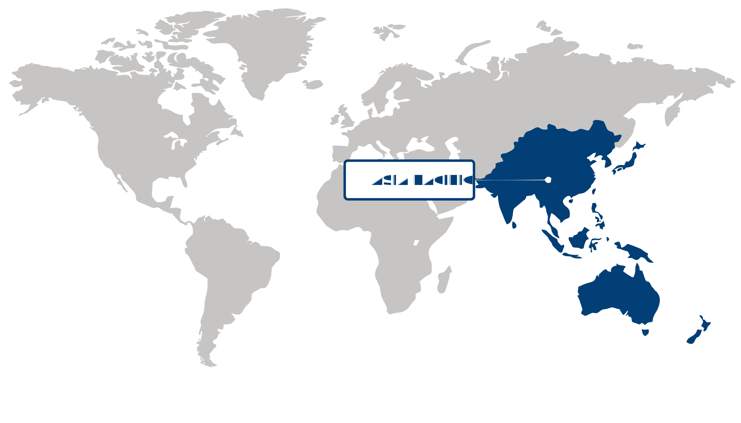
captured over 44.28% of the global market in 2025 and expanding at a 10.5% CAGR, Asia Pacific is the largest and fastest-growing region in the backside illuminated (BSI) CMOS image sensor market. This leadership stems from an extensive, world-dominating semiconductor ecosystem—fab scale and advanced process leadership from Taiwan Semiconductor Manufacturing Company (TSMC), imaging R&D and product leadership at Sony Semiconductor Solutions, and system-level demand from Samsung Electronics and major OEMs—supported by industrial policy from the Ministry of Economy, Trade and Industry (METI) in Japan and capacity and technology initiatives by the Ministry of Industry and Information Technology (MIIT) of China. Evidence includes TSMC announcements on capacity expansion and Sony Semiconductor Solutions product roadmaps. Given dense supply chains, proximity to major smartphone and automotive OEMs, and active public-private investment, Asia Pacific offers sustained opportunity for BSI sensor innovators and upstream suppliers.
Japan is positioned as a pivotal hub in Asia Pacific for the backside illuminated (BSI) CMOS image sensor market, anchoring high-value sensor design and system integration. Sony Semiconductor Solutions remains a global leader in high-performance CMOS image sensors and has publicly detailed product and technology roadmaps that emphasize backside-illuminated and stacked architectures; METI-sponsored R&D and collaborations with automotive manufacturers reinforce Japan’s role in premium imaging for automotive, industrial vision, and professional cameras. Strong IP, manufacturing-grade suppliers such as Nikon and Canon supply chains, and corporate partnerships drive higher ASPs and margin opportunities. Strategically, Japan’s specialization in premium sensors strengthens regional value chains and offers partners differentiated, high-margin product pathways.
China anchors the Asia Pacific expansion of the backside illuminated (BSI) CMOS image sensor market through massive end-market demand and rapid domestic capability building. Domestic players such as Semiconductor Manufacturing International Corporation (SMIC), Sunny Optical, and system customers like Huawei, Xiaomi, Oppo, and Vivo, together with MIIT policy support and initiatives tied to Made in China 2025, have driven localized capacity, packaging, and integration. Company announcements from Sunny Optical and capacity plans at SMIC illustrate growing domestic supply. China’s scale in smartphone shipments, surveillance, and automotive electronics creates volume pull that complements Japan’s premium focus and Taiwan’s foundry strengths, making China a core growth engine for scale suppliers and technology adopters across the region.
North America Market Analysis:
North America held a substantial share in the backside illuminated (BSI) CMOS image sensor market, supported by concentrated OEM demand, expanding fabrication capacity, and deep R&D ecosystems. Robust device and automotive camera adoption from leading buyers and surveillance upgrade cycles sustain volume demand, while policy support such as the White House CHIPS and Science Act and investment activity reported by the Semiconductor Industry Association underpin onshore capacity growth. Announcements by TSMC and Intel to expand U.S. fabs, together with established imaging suppliers like OmniVision Technologies and onsemi maintaining design and production footprints, provide practical evidence of supply-side scaling. These dynamics—large enterprise procurement, proximity to systems integrators, and government-backed manufacturing incentives—position the region for continued strategic opportunity in higher-value BSI implementations across mobile, automotive, and industrial segments.
U.S. serves as the design and systems hub in the backside illuminated (BSI) CMOS image sensor market, concentrating platform-level innovation and large OEM procurement. Apple’s multi-camera iPhone roadmaps and Qualcomm’s imaging ISP integrations drive premium sensor requirements, while U.S.-based suppliers such as OmniVision Technologies and onsemi maintain product and application engineering close to key customers; the U.S. Department of Commerce’s CHIPS-era funding programs further lower deployment risk for localized capacity. This combination of lead-system design, software-enabled image-processing expertise, and policy-backed manufacturing expansion creates a strategic pathway for suppliers to capture high-margin BSI projects and accelerate regional adoption across consumer, automotive, and industrial use cases.
Europe Market Trends:
Experienced lucrative growth in the backside illuminated (BSI) CMOS image sensor market across North America as converging consumer and industrial demand has pushed adoption beyond mobile into automotive and industrial vision; evidence includes the White House’s CHIPS and Science Act commitments (The White House) that underwrite domestic capacity and Sony Semiconductor Solutions’ recent product disclosures demonstrating stacked BSI advancements (Sony Semiconductor Solutions Corporation), while Apple’s camera feature roadmaps (Apple) and OmniVision Technologies announcements (OmniVision Technologies) highlight escalating end-market requirements. Supply-chain reshoring, higher capital intensity, and growing commercial procurement signal sizable investor opportunity in differentiated BSI technology and localized manufacturing capacity.
The United States occupies a leading role in the backside illuminated (BSI) CMOS image sensor market driven by policy incentives and high-value customer demand, with direct support from the U.S. Department of Commerce’s CHIPS initiatives (U.S. Department of Commerce) and mission-led procurements such as NASA sensor programs (National Aeronautics and Space Administration). Corporate R&D and M&A activity—illustrated by ON Semiconductor and Teledyne Technologies press releases on imaging platforms (ON Semiconductor; Teledyne Technologies)—favors premium BSI segments, implying that investors prioritizing fabrication scale-ups and defense/space-qualified roadmaps can capture outsized returns.
Canada serves as a focused innovation hub in the backside illuminated (BSI) CMOS image sensor market where specialty suppliers and public research translate into industrial-grade deployments; Teledyne DALSA’s sensor business growth (Teledyne DALSA) and collaborative projects with the National Research Council Canada (National Research Council Canada) exemplify this pathway, supported by targeted funding from Innovation, Science and Economic Development Canada. Niche strengths in machine vision, medical imaging, and automation create strategic entry points for partners and investors aiming to leverage Canadian IP and supply-chain nodes to complement broader North American scaling.
| Parameter | North America | Asia Pacific | Europe | Latin America | MEA |
|---|---|---|---|---|---|
| Innovation Hub i Scale Nascent Developing Advanced | |||||
| Cost-Sensitive Region i Scale Low Medium High | |||||
| Regulatory Environment i Scale Restrictive Neutral Supportive | |||||
| Demand Drivers i Scale Weak Moderate Strong | |||||
| Development Stage i Scale Emerging Developing Developed | |||||
| Adoption Rate i Scale Low Medium High | |||||
| New Entrants / Startups i Scale Sparse Moderate Dense | |||||
| Macro Indicators i Scale Weak Stable Strong |
Segment Leadership and Growth Trends
Backside Illuminated (BSI) CMOS Image Sensor Market Share (%), by Type, 2026
Go beyond the chart, access full insights & data tables
Request Free Sample ReportMore than 10 Megapixels dominated the backside illuminated (BSI) CMOS image sensor market in 2025, driven by strong demand for high-resolution imaging across smartphones, automotive ADAS and surveillance applications. This segment leads because manufacturers and OEMs seek finer-detail capture to support computational photography, object detection and forensic-grade video, a trend underscored by Sony Semiconductor Solutions and Samsung Electronics product announcements highlighting high‑megapixel BSI sensors for mobile and security use; Hikvision's rollout of 4K/8MP surveillance cameras further illustrates adoption. Preference for richer imagery, edge-AI requirements, and supply‑chain investments in advanced fabs create openings for incumbents to scale and for specialized entrants to offer optimized modules, and ongoing camera-centric product roadmaps suggest sustained relevance near term.
Analysis by Application
Consumer Electronics represented largest share of the backside illuminated (BSI) CMOS image sensor market in 2025, reflecting accelerating smartphone penetration and demand for advanced imaging features. Leadership stems from handset makers prioritizing low‑light performance, multi‑camera arrays and sensor‑ISP co‑design—evidenced by Apple iPhone camera feature launches, Samsung Electronics smartphone sensor releases, and Qualcomm platform support for computational imaging. Shifts in user behavior toward social video, AR experiences and energy‑efficient designs, plus retailer and carrier bundling strategies, create strategic openings for established sensor suppliers and software‑centric newcomers; integrated hardware–software roadmaps and continued smartphone innovation imply this application will stay central in the near to mid term.
| Segment | Sub-Segment | Largest Segment | Fastest Growing |
|---|---|---|---|
| Type | More than 10 Megapixels, 5 to 10 Megapixels, Less than 5 Megapixels | ||
| Application | Security, Medical, Industrial, Automotive, Consumer Electronics |
Competitive Landscape and Market Positioning
The competitive landscape is marked by intensified strategic activity as incumbents strengthen customer linkages, secure capacity through selective consolidation, refresh product roadmaps toward stacked-BSI and larger-pixel architectures, and accelerate investments in process and packaging. These initiatives sharpen differentiation around low-light performance, power efficiency, and system-level integration while raising entry barriers for smaller entrants. As a result, foundry collaboration and IP licensing increasingly determine time-to-market and margin capture across segments.
Strategic / Actionable Recommendations for Regional Players
Prioritize alliances with automotive OEMs and cloud-AI platform providers to embed advanced sensor capabilities into end systems; emphasize AI-friendly pixel designs and closer co-development with domestic foundries to shorten iteration cycles and capture industrial and autonomy opportunities.
Leverage proximity to consumer electronics and module ecosystems by expanding collaborative manufacturing arrangements and accelerating node and packaging advances; focus on high-volume mobile and emerging camera applications while protecting margins through proprietary system-level features.
Concentrate on differentiated sensors for automotive safety, industrial automation, and scientific instrumentation by engaging regional research consortia and specialty foundries; strengthen optics integration and quality-assurance pathways to defend premium, regulation-sensitive segments.
| Company | Market Share | Company Revenue | Revenue CAGR (%) | Product Portfolio | Geographic Presence | Innovation / R&D Focus | Strategic Developments |
|---|---|---|---|---|---|---|---|
| No companies available. | |||||||
Industry Development/News
| Company Name | Date | Key Development |
|---|
Customize Your Report
Explore examples of how this report can be tailored to different research needs, including custom segments, additional topics or chapters, and related reports. Click a section of the wheel or its numbered marker to explore the available options.
Backside Illuminated (BSI) CMOS Image Sensor Market — Custom Segments
| Segment | Sub-Segment |
|---|---|
| No segment data available. | |
Backside Illuminated (BSI) CMOS Image Sensor Market — Custom TOC
| Custom Chapter | Custom Details | ||
|---|---|---|---|
| No custom TOC data available. | |||
Need a different cut of the data?
Request Custom ResearchWhat is the market valuation of backside illuminated CMOS image sensor?
How much is the backside illuminated (BSI) CMOS image sensor industry expected to grow by 2035?
In which region is the backside illuminated (BSI) CMOS image sensor market share the greatest?
Which region shows the most rapid acceleration in the backside illuminated CMOS image sensor sector?
When did more than 10 megapixels sub-segment emerge as the largest sub-segment in the type segment of backside illuminated (BSI) CMOS image sensor sector?
Why is the consumer electronics segment leading in the backside illuminated (BSI) CMOS image sensor industry?
Which companies dominate the backside illuminated (BSI) CMOS image sensor landscape?
Our Clients
"Working with FBI has been a good experience. The market report provided a holistic view, covering everything from emerging trends to potential risks."
Semtech Corporation
"The experience was highly positive. The team showcased remarkable flexibility in adapting to our specific needs and delivered report that perfectly aligned with all our requirements."
TSMC
"What really stood out to me was how clearly and promptly the Fundamental Business Insights team communicated throughout. It made the collaboration feel effortless."
NXP Semiconductors
Our Research Team & Methodology
Every Fundamental Business Insights report is built by a dedicated vertical research team, validated through a structured primary-and-secondary methodology, and reviewed for accuracy before it reaches you.
Research Team Overview
Prepared by the Electronics & Semiconductors Research Team
Delivery
Published
Demand
Available
Support
Trust & Compliance
Research Domains
10 coverage areasResearch Intelligence
| Source | Reference |
|---|---|
| Semiconductor Industry Association (SIA) | www.semiconductors.org |
| SEMI | www.semi.org |
| JEDEC Solid State Technology Association | www.jedec.org |
| IEEE | www.ieee.org |
| IPC – Association Connecting Electronics Industries | www.ipc.org |
| International Electrotechnical Commission (IEC) | www.iec.ch |
| International Organization for Standardization (ISO) | www.iso.org |
| U.S. Bureau of Industry and Security (BIS) | www.bis.gov |
| U.S. Patent and Trademark Office (USPTO) | www.uspto.gov |
| European Patent Office (EPO) | www.epo.org |
| Taiwan Semiconductor Industry Association (TSIA) | www.tsia.org.tw |
| World Semiconductor Trade Statistics (WSTS) | www.wsts.org |
| International Energy Agency (IEA) | www.iea.org |
| GSMA | www.gsma.com |
| 3GPP | www.3gpp.org |
| ITU (International Telecommunication Union) | www.itu.int |
| Omdia (public insights) | omdia.tech.informa.com |
| Display Supply Chain Consultants (DSCC) | www.displaysupplychain.com |
| U.S. Department of Energy (DOE) | www.energy.gov |
| NIST (National Institute of Standards and Technology) | www.nist.gov |
Research Workflow & Quality Assurance
Data Collection
Verified information gathered through primary and secondary research.
Data Triangulation
Cross-validation using multiple independent data sources.
Forecast Modelling
Market estimates developed using historical trends and analytical models.
Analyst Validation
Findings reviewed by domain experts for accuracy and consistency.
Editorial & Quality Review
Final editorial, quality, and compliance checks before publication.
Final Publication
Released after successful completion of the internal review process.
Report Coverage
📊 Market Assessment
- Market Size & Forecast
- Market Segmentation
- Regional Analysis
- Growth Drivers & Challenges
- Market Dynamics
🏢 Competitive Intelligence
- Competitive Landscape
- Company Profiles
- Competitive Benchmarking
- Mergers & Acquisitions
- Market Share Analysis or Key Company Strategies
🔍 Strategic Analysis
- Value Chain Analysis
- Porter's Five Forces
- PESTLE Analysis
- Pricing Trends
- Supply-Demand Analysis
🚀 Future Outlook
- Technology Landscape
- Regulatory Landscape
- Investment & Funding Landscape
- Emerging Opportunities
- Future Market Outlook
Have a question about this report or need a custom scope?
Request Customization