Atomic Layer Deposition Market Size & Forecasts 2026-2035, By Segments (Product, Application), Growth Opportunities, Innovation Landscape, Regulatory Shifts, Strategic Regional Insights (U.S., Japan, China, South Korea, UK, Germany, France), and Competitive Dynamics (ASM International, Tokyo Electron, Lam Research, Applied Materials, Veeco)
Market Size and Growth Outlook
Atomic Layer Deposition Market size is predicted to expand from USD 2.79 billion in 2025 to USD 9.22 billion by 2035, with growth underpinned by a CAGR above 12.7% between 2026 and 2035. The industry revenue outlook for 2026 is USD 3.1 billion.
Get more details on this report
Request Free Sample ReportAtomic Layer Deposition Market Intelligence Snapshot
Regional Market Dynamics
Segment Momentum
Market Expansion Drivers
Leading Market Participants
Global Market Forecast Snapshot
Market Outlook
Regional and Segment Outlook
Market Growth Drivers and Industry Trends
The surge in advanced-node devices and heterogeneous integration is directly expanding the atomic layer deposition market because ALD enables high-conformality films for gate stacks, interconnect barriers, and 3D structures. Announcements from TSMC and Intel about advanced-node capacity and packaging investments, together with equipment roadmaps from Applied Materials and Lam Research, provide qualitative evidence that fabs are prioritizing ALD-capable toolchains. Established toolmakers can capture value by bundling ALD modules into turnkey fabs and long-term service contracts, while new entrants can win niche business supplying precursors, retrofit modules, or application-specific processes. Observed fab commitments and vendor roadmaps point to sustained ALD integration across future logic and packaging lines.
Adoption in advanced coating and thin-film applications
Broader use of ALD in optics, MEMS, and energy devices is diversifying end markets and driving industrialization of the atomic layer deposition market as it moves beyond pure-semiconductor use cases. Research outcomes from the National Renewable Energy Laboratory (NREL) and pilot projects at Fraunhofer institutes demonstrate ALD’s role in improving battery electrodes and anti-reflective optical coatings, while equipment providers like Oxford Instruments and Picosun report shipments to research and industrial customers. Incumbent suppliers can leverage channel relationships to cross-sell ALD services into adjacent sectors; startups can specialize in precursor chemistries or contract coating services. Ongoing cross-sector pilots and published R&D show a clear path from lab validation to commercial deployments.
Innovations in ALD equipment and process efficiency
Advances in spatial ALD, precursor delivery, and in-situ process control are raising throughput and enabling new applications, directly shaping the atomic layer deposition market by reducing per-unit cost and cycle time. Press releases and technical briefings from ASM International, Applied Materials, and Picosun emphasize tool architectures and process modules that improve footprint and uniformity, while SEMI discussions highlight industry interest in standardizing metrics for throughput and reliability. Large suppliers can monetize these innovations through platform upgrades and software-enabled services; new entrants can compete with specialized modules, control software, or novel precursor technologies. The current cadence of vendor tool announcements and standards work indicates incremental but practical efficiency gains on production lines.
Industry Restraints:
High Capital Intensity and Throughput Constraints
Atomic layer deposition’s slow cycle times and high-cost vacuum and precursor delivery systems make tool CAPEX and fab integration a persistent bottleneck, limiting rapid adoption in high-volume manufacturing. SEMI has documented prolonged equipment lead times that compound investment risk, while equipment vendors such as Applied Materials and ASM International have publicly emphasized development of higher-throughput ALD platforms to address demand. For incumbents, this drives large upfront spending and long qualification cycles; for new entrants, it raises financial and operational barriers to scale. Near to medium term, market structure will favor vendors and fabs that can amortize expensive ALD platforms and deliver validated, higher-throughput solutions.
Precursor Availability and Regulatory Restrictions
The ALD value chain depends on a narrow set of highly specialized precursors whose synthesis, handling and disposal are subject to tightening regulation, constraining material options and slowing process qualification. European Chemicals Agency (ECHA) actions on PFAS and the U.S. Environmental Protection Agency (EPA) reviews under TSCA have increased scrutiny on fluorinated and metalorganic precursors, while specialty suppliers such as Strem Chemicals and BASF remain critical sources. This raises costs and lengthens qualification for both tool vendors and chipmakers; smaller fabs and startups face greater supply and compliance risk. Expect continued regulatory-driven conservatism and supplier consolidation to favor established players that can secure compliant, long-term precursor supply.
| Growth Driver | Impact on CAGR | Regulatory Influence | Geographic Relevance | Adoption Rate | Impact Timeline |
|---|---|---|---|---|---|
| Increasing demand in semiconductor and electronics industries | 4.00% | Short term (≤ 2 yrs) | North America, Asia Pacific | Medium | Fast |
| Adoption in advanced coating and thin-film applications | 3.00% | Medium term (2–5 yrs) | Europe, North America | Low | Moderate |
| Innovations in ALD equipment and process efficiency | 2.00% | Long term (5+ yrs) | Asia Pacific, Europe | Medium | Moderate |
Unlock insights tailored to your business with our bespoke market research solutions.
Click to get your customized report now.
Regional Demand Dynamics
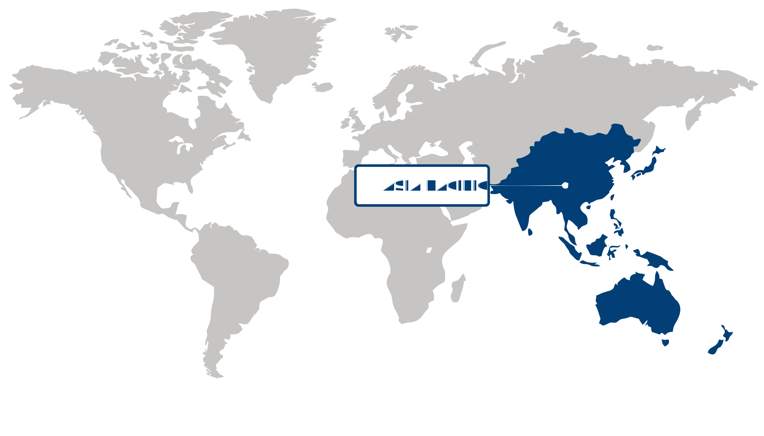
The Asia Pacific region captured over 41.8% of the global atomic layer deposition market in 2025 and is the largest regional market, driven chiefly by a booming semiconductor and advanced electronics manufacturing base. Support for this leadership is visible in public announcements by Taiwan Semiconductor Manufacturing Company (TSMC) and Samsung Electronics regarding capacity expansions, and in SEMI reporting elevated wafer fab equipment demand into APAC. Policy backing from Japan’s Ministry of Economy, Trade and Industry (METI) and China’s Ministry of Industry and Information Technology (MIIT) further accelerates investment in advanced node fabs and packaging, while suppliers such as Tokyo Electron Limited are scaling deposition tool capabilities. These dynamics—strong OEM demand, government incentives, and equipment-supplier innovation—position APAC to capture higher-value ALD adoption across logic, memory, and specialty electronics over the coming investment cycles.
Japan is positioned as a pivotal hub in Asia Pacific for the atomic layer deposition market, leveraging a dense ecosystem of equipment OEMs, materials producers, and targeted industrial policy. Tokyo Electron Limited and other Japanese equipment suppliers have highlighted tool roadmaps and performance upgrades in corporate releases, and METI’s semiconductor initiatives have prioritized local supply-chain resilience and advanced materials sourcing. Domestic strengths in precision manufacturing and a skilled workforce mean Japan will be a center for advanced-node ALD process adoption and collaborative R&D with global foundries, reinforcing broader regional technology leadership.
China anchors the regional expansion for the atomic layer deposition market, supported by large-scale fab investments and industrial-policy coordination. Public signals from the Ministry of Industry and Information Technology (MIIT) and activity reported by firms such as Semiconductor Manufacturing International Corporation (SMIC) and Yangtze Memory Technologies reflect prioritization of memory and logic capacity growth; the China Semiconductor Industry Association also documents rising domestic equipment and materials programs. High-volume demand from local IDM and foundry customers, coupled with government-backed capital projects, creates sizeable near-term ALD equipment and consumables opportunities that complement Japan’s tooling strengths and strengthen APAC’s overall market gravity.
North America Market Analysis:
North America emerged as the fastest-growing region in the atomic layer deposition market, registering a CAGR of 15.2%. Growth is driven by heavy capex and R&D in semiconductor fabs and advanced packaging, spurring demand for high‑precision ALD tooling and services. Policy support from the U.S. CHIPS and Science Act and targeted funding via the U.S. Department of Commerce accelerate fabrication build-outs, while announcements by Intel and TSMC on new U.S. fabs validate near‑term tool demand. Equipment vendors such as Applied Materials and Lam Research have signaled expanded ALD roadmaps in corporate releases, reflecting supplier readiness. These dynamics create concentrated opportunities across tools, precursors, and collaborative process development.
The U.S. anchors the atomic layer deposition market in North America as the primary beneficiary of fab capex and advanced‑packaging R&D, translating incentives into procurement cycles. Intel’s investments in Ohio and Arizona and TSMC’s Arizona commitments have driven localized demand for ALD systems and specialized process expertise, while Applied Materials and Lam Research corporate announcements cite U.S. collaborations with fabs and packaging houses. Procurement preferences favor suppliers offering integrated tool‑to‑process solutions and development support; university and DOE/NSF linkages strengthen skilled talent supply. Strategically, strong U.S. demand creates reference fabs and scale effects that accelerate adoption and supplier consolidation across the region.
Europe Market Trends:
Held a substantial share, Europe’s position in the atomic layer deposition market is anchored by a dense semiconductor ecosystem, targeted public programs, and deep research capabilities that together sustain commercial demand and advanced-node process development. Evidence includes the European Commission’s IPCEI on Microelectronics and European Investment Bank project financing for fabs, Fraunhofer-Gesellschaft and CEA-Leti publications on thin-film processes, and equipment orders reported by ASM International and Oxford Instruments. These linked capabilities—clustered suppliers, large industrial buyers, and coordinated funding—create scalable adoption pathways and meaningful opportunities for toolmakers, materials suppliers, and specialized service providers across the region.
Germany serves as a manufacturing and systems-integration leader in the atomic layer deposition market, driven by strong automotive and power-semiconductor demand and a high concentration of equipment buyers. Infineon Technologies’ capacity expansion announcements and Fraunhofer-Gesellschaft applied research on ALD-enabled dielectric and barrier layers illustrate commercial pull and technical maturation, while the Federal Ministry for Economic Affairs and Climate Action (BMWK) programs and regional supplier networks reduce deployment friction. For vendors and investors, Germany’s production scale and embedded supply chains make it a priority market for repeatable industrial engagements.
France occupies a strategic research-and-materials niche in the atomic layer deposition market, propelled by national innovation labs and specialty-material firms that accelerate upstream technology adoption. CEA-Leti’s research on ALD integration, Soitec’s substrate developments, and Bpifrance-supported initiatives linked to STMicroelectronics demonstrate a research-to-manufacturing pathway favoring specialty ALD applications in power and RF segments. That combination positions France as an attractive trial and scale-up environment for novel precursors, process flows, and collaborative commercialization across European clusters.
| Parameter | North America | Asia Pacific | Europe | Latin America | MEA |
|---|---|---|---|---|---|
| Innovation Hub i Scale Nascent Developing Advanced | |||||
| Cost-Sensitive Region i Scale Low Medium High | |||||
| Regulatory Environment i Scale Restrictive Neutral Supportive | |||||
| Demand Drivers i Scale Weak Moderate Strong | |||||
| Development Stage i Scale Emerging Developing Developed | |||||
| Adoption Rate i Scale Low Medium High | |||||
| New Entrants / Startups i Scale Sparse Moderate Dense | |||||
| Macro Indicators i Scale Weak Stable Strong |
Segment Leadership and Growth Trends
Atomic Layer Deposition Market Share (%), by Product, 2026
Go beyond the chart, access full insights & data tables
Request Free Sample ReportThermal ALD dominated the atomic layer deposition market in 2025 as the largest share within product segments, driven by its proven reliability and superior film quality in high-volume semiconductor production. Applied Materials and Lam Research have publicized deployments of thermal-ALD-capable tools for production fabs, while equipment suppliers such as Oxford Instruments and Picosun emphasize uniformity and throughput advantages, reflecting customer preference for process robustness. This leadership opens strategic opportunities for incumbent toolmakers, precursor suppliers and specialist service providers to scale offerings, and for new entrants to target niche materials and retrofit services. Given ongoing node scaling, packaging demands and supply-chain maturation, thermal ALD is poised to remain central in the near to medium term.
Analysis by Application
Electronics & Semiconductors represented largest share of the atomic layer deposition market in 2025 among application segments, propelled by continuous device scaling and rising demand for advanced chips. The International Roadmap for Devices and Systems (IRDS) and SEMI roadmaps highlight ALD adoption for conformal films in advanced nodes and packaging; TSMC and Intel roadmaps also underscore ALD in critical patterning and gate-stack processes. End-user demand for performance, yield and sustainability is shifting procurement toward ALD-enabled process steps, creating openings for foundries, OSATs and materials innovators. As heterogeneous integration and tighter device tolerances persist, this application segment should retain strategic relevance through the near to medium term.
| Segment | Sub-Segment | Largest Segment | Fastest Growing |
|---|---|---|---|
| Product | Thermal ALD, Metal ALD, Plasma-Enhanced ALD | ||
| Application | Electronics & Semiconductors, Medical, Solar Devices |
Competitive Landscape and Market Positioning
The competitive landscape is characterized by targeted portfolio expansion, intensified co-development with leading fabs, and selective consolidation that tightens supplier ecosystems. Firms are introducing differentiated tool capabilities, enhancing in-tool analytics, and aligning with precursor and metrology partners to accelerate qualification; such moves reinforce barriers to entry, shift competitive advantage toward integrated solution providers, and enable faster adoption in adjacent segments like power devices and photonics. Smaller, agile vendors leverage specialization to preserve competitive footholds and trigger focused responses from incumbents.
Strategic / Actionable Recommendations for Regional Players
Prioritize deeper collaboration with local foundries and integrated device manufacturers, expand retrofit and upgrade services, and integrate automation and data-driven process control to shorten qualification timelines and capture adjacent opportunities.
Scale regional R&D linkages and manufacturing capacity while aligning with supplier consortia to secure precursor and component continuity; emphasize high-volume node support and close co-development with major fabs to strengthen market position.
Focus on specialty thin-film and niche end markets by partnering with research institutions and instrument providers, adopting greener chemistries, and tailoring solutions for MEMS, photonics, and compound-semiconductor applications to differentiate from large global incumbents.
| Company | Market Share | Company Revenue | Revenue CAGR (%) | Product Portfolio | Geographic Presence | Innovation / R&D Focus | Strategic Developments |
|---|---|---|---|---|---|---|---|
| No companies available. | |||||||
Industry Development/News
| Company Name | Date | Key Development |
|---|
Customize Your Report
Explore examples of how this report can be tailored to different research needs, including custom segments, additional topics or chapters, and related reports. Click a section of the wheel or its numbered marker to explore the available options.
Atomic Layer Deposition Market — Custom Segments
| Segment | Sub-Segment |
|---|---|
| No segment data available. | |
Atomic Layer Deposition Market — Custom TOC
| Custom Chapter | Custom Details | ||
|---|---|---|---|
| No custom TOC data available. | |||
Need a different cut of the data?
Request Custom ResearchWhat is the market valuation of atomic layer deposition?
What are the growth projections for the atomic layer deposition industry?
What is the leading region in terms of atomic layer deposition market share?
What region has posted the highest CAGR in the atomic layer deposition sector?
Why does thermal ALD sub-segment dominate the product segment of atomic layer deposition sector?
How does electronics & semiconductors segment fare in the atomic layer deposition industry?
Which companies dominate the atomic layer deposition landscape?
Our Clients
"Working with FBI has been a good experience. The market report provided a holistic view, covering everything from emerging trends to potential risks."
Semtech Corporation
"The experience was highly positive. The team showcased remarkable flexibility in adapting to our specific needs and delivered report that perfectly aligned with all our requirements."
TSMC
"What really stood out to me was how clearly and promptly the Fundamental Business Insights team communicated throughout. It made the collaboration feel effortless."
NXP Semiconductors
Our Research Team & Methodology
Every Fundamental Business Insights report is built by a dedicated vertical research team, validated through a structured primary-and-secondary methodology, and reviewed for accuracy before it reaches you.
Research Team Overview
Prepared by the Electronics & Semiconductors Research Team
Delivery
Published
Demand
Available
Support
Trust & Compliance
Research Domains
10 coverage areasResearch Intelligence
| Source | Reference |
|---|---|
| Semiconductor Industry Association (SIA) | www.semiconductors.org |
| SEMI | www.semi.org |
| JEDEC Solid State Technology Association | www.jedec.org |
| IEEE | www.ieee.org |
| IPC – Association Connecting Electronics Industries | www.ipc.org |
| International Electrotechnical Commission (IEC) | www.iec.ch |
| International Organization for Standardization (ISO) | www.iso.org |
| U.S. Bureau of Industry and Security (BIS) | www.bis.gov |
| U.S. Patent and Trademark Office (USPTO) | www.uspto.gov |
| European Patent Office (EPO) | www.epo.org |
| Taiwan Semiconductor Industry Association (TSIA) | www.tsia.org.tw |
| World Semiconductor Trade Statistics (WSTS) | www.wsts.org |
| International Energy Agency (IEA) | www.iea.org |
| GSMA | www.gsma.com |
| 3GPP | www.3gpp.org |
| ITU (International Telecommunication Union) | www.itu.int |
| Omdia (public insights) | omdia.tech.informa.com |
| Display Supply Chain Consultants (DSCC) | www.displaysupplychain.com |
| U.S. Department of Energy (DOE) | www.energy.gov |
| NIST (National Institute of Standards and Technology) | www.nist.gov |
Research Workflow & Quality Assurance
Data Collection
Verified information gathered through primary and secondary research.
Data Triangulation
Cross-validation using multiple independent data sources.
Forecast Modelling
Market estimates developed using historical trends and analytical models.
Analyst Validation
Findings reviewed by domain experts for accuracy and consistency.
Editorial & Quality Review
Final editorial, quality, and compliance checks before publication.
Final Publication
Released after successful completion of the internal review process.
Report Coverage
📊 Market Assessment
- Market Size & Forecast
- Market Segmentation
- Regional Analysis
- Growth Drivers & Challenges
- Market Dynamics
🏢 Competitive Intelligence
- Competitive Landscape
- Company Profiles
- Competitive Benchmarking
- Mergers & Acquisitions
- Market Share Analysis or Key Company Strategies
🔍 Strategic Analysis
- Value Chain Analysis
- Porter's Five Forces
- PESTLE Analysis
- Pricing Trends
- Supply-Demand Analysis
🚀 Future Outlook
- Technology Landscape
- Regulatory Landscape
- Investment & Funding Landscape
- Emerging Opportunities
- Future Market Outlook
Have a question about this report or need a custom scope?
Request Customization