Chemical Vapor Deposition (CVD) Market Size & Growth Forecast 2027–2036, By Segments (Category, Application), Regional Demand Trends (North America, Asia Pacific, Europe), Key Country Insights (U.S., Japan, South Korea, Germany, France, Italy), and Competitive Landscape
Market Size and Growth Outlook
Chemical Vapor Deposition Market size was estimated at USD 28.6 billion in 2026 and is projected to grow at a 9.03% CAGR from 2027 to 2036, surpassing USD 67.89 billion by 2036. The industry revenue for 2027 is assessed at USD 30.77 billion.
Get more details on this report
Request Free Sample ReportChemical Vapor Deposition (CVD) Market Intelligence Snapshot
Regional Market Dynamics
- Asia Pacific held a 54.71% market share in 2026, driven by its concentration of semiconductor, electronics, and advanced materials manufacturing that relies heavily on commercial-scale CVD processes.
- Asia Pacific is projected to expand at a 10.4% CAGR as manufacturers increase fabrication capacity, improve process precision, and support growing demand for high-performance devices.
Segment Momentum
- CVD Equipment held a 63.34% share in 2026 because deposition tools are essential production assets that provide process control, film uniformity, and consistent throughput across manufacturing operations.
- Medical Equipment is the fastest-growing application segment as demand rises for advanced surface coatings that improve durability, biocompatibility, and performance stability in specialized medical components.
Market Expansion Drivers
- Semiconductor miniaturization and advanced microelectronics driving precision thin-film deposition demand.
- Expanding applications in solar, optics, and medical devices boosting CVD utilization.
- Asia Pacific manufacturing expansion and India semiconductor growth accelerating CVD adoption.
Leading Market Participants
- Top players in the chemical vapor deposition market include Applied Materials, Inc. (United States), ASM International N.V. (Netherlands), Tokyo Electron Limited (Japan), Veeco Instruments Inc. (United States), Aixtron SE (Germany), CVD Equipment Corporation (United States), ULVAC, Inc. (Japan), Oxford Instruments plc (United Kingdom), OC Oerlikon Management AG (Switzerland), IHI Corporation (Japan).
Global Market Forecast Snapshot
Market Outlook
- 2026 Market Size: USD 28.6 billion
- 2027 Estimated Market Size: USD 30.77 billion.
- Projected Market Size: USD 67.89 billion by 2036
- Growth Forecast: 9.03% CAGR (2027-2036)
Regional and Segment Outlook
- Leading Regional Market: Asia Pacific
- High-Growth Regional Hub: Asia Pacific
- Core Revenue Segment: CVD Equipment (Category) | Semiconductor & Microelectronics (Application)
- Emerging Opportunity Segment: CVD Services (Category) | Medical Equipment (Application)
Market Growth Drivers and Industry Trends
Semiconductor miniaturization and advanced microelectronics driving precision thin-film deposition demand
Continued semiconductor miniaturization is creating strong requirements for highly controlled thin-film formation, supporting the chemical vapor deposition market across advanced microelectronics manufacturing. As electronic components become smaller and more densely integrated, manufacturers require deposition processes capable of producing uniform films with precise thickness and material properties on complex structures. CVD technologies provide controlled deposition capabilities for a range of functional materials used in semiconductor fabrication, supporting the development of sophisticated devices where surface quality, layer uniformity, and process consistency are critical.
Expanding applications in solar, optics, and medical devices boosting CVD utilization
Diversification beyond semiconductor fabrication is broadening the application base of the chemical vapor deposition market as industries increasingly use engineered thin films to improve component performance. In solar technologies, deposited materials can contribute to functional layers and surface properties, while optical applications use specialized coatings and materials to achieve desired transmission, reflection, or durability characteristics. Medical devices can also benefit from CVD-based coatings that enhance surface performance, wear resistance, or biocompatibility, creating demand for deposition capabilities tailored to specialized component requirements.
Asia Pacific manufacturing expansion and India semiconductor growth accelerating CVD adoption
Rapid expansion of manufacturing infrastructure across asia pacific is strengthening the chemical vapor deposition market by increasing regional demand for advanced production equipment and materials. Semiconductor manufacturing growth in india is adding to this momentum as investments in domestic electronics and chip production create requirements for specialized fabrication processes. The development of local manufacturing ecosystems can also encourage supporting investments in deposition capabilities, process engineering, and related semiconductor infrastructure, increasing the integration of CVD technologies within regional production facilities.
| Growth Driver | Impact on CAGR | Regulatory Influence | Geographic Relevance | Adoption Rate | Impact Timeline |
|---|---|---|---|---|---|
| Semiconductor miniaturization and advanced microelectronics driving precision thin-film deposition demand | 2.30% | High | Asia Pacific | High | Near Term |
| Expanding applications in solar, optics, and medical devices boosting CVD utilization | 2.00% | Moderate | North America, Europe | Medium | Mid Term |
| Asia Pacific manufacturing expansion and India semiconductor growth accelerating CVD adoption | 1.70% | Moderate | Asia Pacific | High | Mid Term |
Unlock insights tailored to your business with our bespoke market research solutions.
Click to get your customized report now.
Regional Demand Dynamics
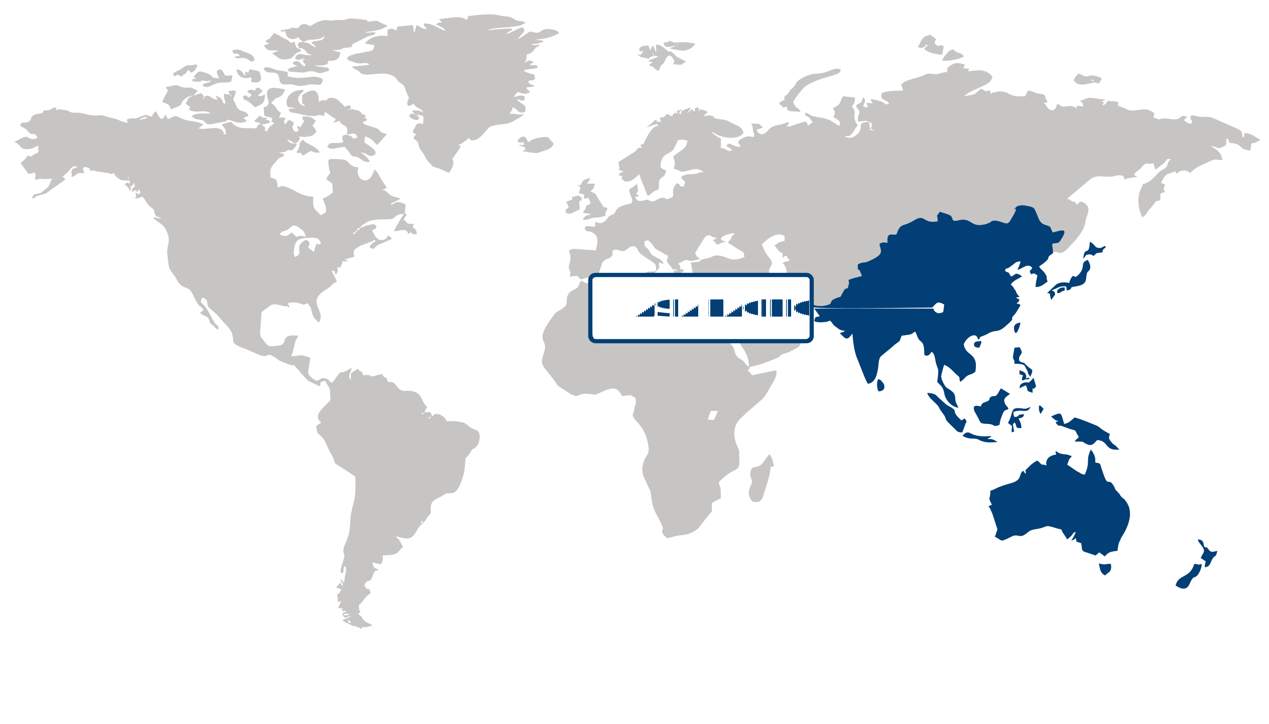
Asia Pacific (Largest & Fastest-Growing Region)
The chemical vapor deposition market was led by Asia Pacific, which accounted for a 54.71% share in 2026, with the region also representing the fastest-growing market. Its strong position is closely linked to the concentration of semiconductor, electronics, solar, and advanced materials manufacturing, where chemical vapor deposition is essential for producing high-performance coatings and thin films. Expanding semiconductor fabrication capacity and continued investment in sophisticated electronics manufacturing are supporting demand for advanced deposition equipment and materials. At the same time, the development of next-generation chips, high-performance components, and specialized coatings is encouraging manufacturers to adopt increasingly precise deposition processes. Government-backed industrial development initiatives and efforts to strengthen regional technology supply chains further support investment in fabrication infrastructure, creating favorable conditions for continued adoption of chemical vapor deposition technologies.
| Parameter | North America | Asia Pacific | Europe | Latin America | MEA |
|---|---|---|---|---|---|
| Innovation Hub i Scale Nascent Developing Advanced | |||||
| Cost-Sensitive Region i Scale Low Medium High | |||||
| Regulatory Environment i Scale Restrictive Neutral Supportive | |||||
| Demand Drivers i Scale Weak Moderate Strong | |||||
| Development Stage i Scale Emerging Developing Developed | |||||
| Adoption Rate i Scale Low Medium High | |||||
| New Entrants / Startups i Scale Sparse Moderate Dense | |||||
| Macro Indicators i Scale Weak Stable Strong |
Key Country Insights
Germany 🇩🇪
Precision Engineering ApplicationsGermany applies chemical vapor deposition extensively across precision engineering, automotive manufacturing, and industrial tooling. Manufacturers in Germany prioritize coating quality, equipment reliability, and advanced material performance for demanding production environments.
France 🇫🇷
Aerospace Coating ExpertiseFrance utilizes chemical vapor deposition across aerospace, electronics, and research-intensive manufacturing activities. Industrial users in France emphasize protective coatings and advanced material performance that improve durability and component reliability.
Italy 🇮🇹
Industrial Surface EnhancementItaly incorporates chemical vapor deposition into industrial equipment, tooling, and specialty manufacturing operations requiring durable surface coatings. Companies in Italy increasingly value deposition technologies that enhance product lifespan and manufacturing precision.
Japan 🇯🇵
High-Performance Materials FocusJapan continues advancing chemical vapor deposition technologies for electronics, optics, and precision component manufacturing. Companies in Japan emphasize process consistency and thin-film quality to support sophisticated industrial and semiconductor applications.
South Korea 🇰🇷
Chip Manufacturing SupportSouth Korea maintains strong demand for chemical vapor deposition equipment through its semiconductor manufacturing ecosystem. Manufacturers in South Korea focus on deposition technologies capable of supporting advanced chip fabrication and high-volume production requirements.
United States 🇺🇸
Advanced Semiconductor FabricationThe U.S. chemical vapor deposition market is driven by semiconductor manufacturing, aerospace components, and advanced materials engineering. Investment across the U.S. continues to emphasize deposition technologies that improve device performance, production precision, and manufacturing efficiency.
Segment Leadership and Growth Trends
Chemical Vapor Deposition (CVD) Market Share (%), by Category, 2026
Go beyond the chart, access full insights & data tables
Request Free Sample ReportCategory Segment Analysis: CVD Equipment (Largest Segment) vs CVD Services (Fastest-Growing Segment)
CVD equipment dominated the chemical vapor deposition (CVD) market, accounting for a 63.34% share in 2026. Its leading position is supported by the essential role of deposition equipment in producing thin films and coatings with controlled thickness, composition, and uniformity across advanced manufacturing processes. Growing demand for semiconductor components, microelectronic devices, advanced materials, and high-performance coatings is encouraging manufacturers to invest in increasingly precise deposition systems. Continued emphasis on process automation, production efficiency, and equipment capabilities is further reinforcing the importance of CVD equipment across technology-intensive industries.
CVD services are emerging as the fastest-growing category as manufacturers increasingly seek specialized deposition capabilities without assuming the full cost and operational complexity associated with maintaining dedicated equipment. Outsourced services can provide access to specialized process expertise, controlled deposition environments, and customized coating capabilities for organizations with varied production requirements. The growing use of CVD processes across emerging applications, combined with demand for flexible manufacturing support, is strengthening the role of specialized service providers.
Application Segment Analysis: Semiconductor & Microelectronics (Largest Segment) vs Medical Equipment (Fastest-Growing Segment)
The semiconductor & microelectronics segment held the largest share of the chemical vapor deposition (CVD) market at 58.39% in 2026. CVD processes are fundamental to the fabrication of advanced electronic components because they enable precise deposition of functional materials used in semiconductor and microelectronic structures. Increasing device complexity and the ongoing development of smaller, higher-performance electronic components are driving demand for controlled thin-film deposition. The expanding role of advanced electronics across computing, communications, automotive systems, and industrial technologies continues to support strong utilization of CVD processes in this application.
Medical equipment represents the fastest-growing application segment as manufacturers increasingly utilize advanced coatings and deposited materials to improve the performance, durability, and functional characteristics of medical components. CVD can support the development of surfaces with specialized properties such as wear resistance, chemical stability, and biocompatibility, depending on the material system and process. Growing demand for sophisticated medical devices and continued innovation in device materials are creating new opportunities for CVD technologies within medical equipment manufacturing.
| Segment | Sub-Segment | Largest Segment | Fastest Growing |
|---|---|---|---|
| Category | CVD Equipment, CVD Materials, CVD Services | CVD Equipment | CVD Services |
| Application | Semiconductor & Microelectronics, Data Storage, Solar Products, Cutting Tools, Medical Equipment, Other | Semiconductor & Microelectronics | Medical Equipment |
Competitive Landscape and Market Positioning
Major players in the chemical vapor deposition (CVD) market:
1. Applied Materials Inc. (United States)
2. ASM International N.V. (Netherlands)
3. Tokyo Electron Limited (Japan)
4. Veeco Instruments Inc. (United States)
5. Aixtron SE (Germany)
6. CVD Equipment Corporation (United States)
7. ULVAC Inc. (Japan)
8. Oxford Instruments plc (United Kingdom)
9. OC Oerlikon Management AG (Switzerland)
10. IHI Corporation (Japan)
The chemical vapor deposition (CVD) market is experiencing increased demand from advanced electronics, semiconductor manufacturing, and high-performance coating applications. Market growth is being supported by ongoing innovation in thin-film deposition technologies that improve material precision, durability, and processing efficiency. Expanding use of advanced coatings in energy storage, aerospace, and microelectronics industries is also driving continuous product development within the chemical vapor deposition (CVD) market.
| Company | Market Share | Company Revenue | Revenue CAGR (%) | Product Portfolio | Geographic Presence | Innovation / R&D Focus | Strategic Developments |
|---|---|---|---|---|---|---|---|
| Applied Materials Inc. (United States) | |||||||
| ASM International N.V. (Netherlands) | |||||||
| Tokyo Electron Limited (Japan) | |||||||
| Veeco Instruments Inc. (United States) | |||||||
| Aixtron SE (Germany) | |||||||
| CVD Equipment Corporation (United States) | |||||||
| ULVAC Inc. (Japan) | |||||||
| Oxford Instruments plc (United Kingdom) | |||||||
| OC Oerlikon Management AG (Switzerland) | |||||||
| IHI Corporation (Japan). |
Industry Development/News
| Company Name | Date | Key Development |
|---|---|---|
| Applied Materials | May-26 | Applied Materials entered into a definitive agreement to acquire ASMPT’s NEXX business, a supplier of large-area advanced packaging deposition equipment. This acquisition expands the company’s panel-level packaging portfolio, strengthening its deposition technology capabilities for next-generation AI semiconductor packaging applications. |
| Centrotherm | Feb-26 | Centrotherm launched the c.Plasma Q Max PECVD system optimized for high-volume TOPCon solar cell manufacturing. Processing up to 10,000 wafers per hour via a single multi-boat chamber, the technology integration aids solar manufacturers transitioning from legacy PERC infrastructure. |
| Graphene Square | Nov-25 | Graphene Square finalized construction of the world’s first mass-production facility for CVD graphene film. The new facility expands manufacturing capacity for specialized graphene materials targeted at advanced electronics and battery sectors, serving as a significant manufacturing milestone for the segment. |
| Kira Jewels | Sep-25 | Kira Jewels scaled its synthetic diamond manufacturing capacity to 250,000 carats per month. The scale-up strengthens the company’s market footprint and addresses escalating industrial and commercial demand for lab-grown gemstones produced via chemical vapor deposition techniques. |
| Element Six | Sep-24 | Element Six and Seki Diamond Systems co-launched the SDS-E600, a compact microwave plasma CVD diamond reactor. The partnership integrates proprietary synthesis technology into an established commercial platform, targeting research institutions to accelerate CVD adoption across the semiconductor, optics, and sensing industries. |
| De Beers | Jun-24 | De Beers announced a strategic shift to cease the production of lab-grown diamonds intended for jewelry applications. This structural operational reallocation from a major participant directly influences competitive dynamics and supply structures within the CVD-grown diamond segment. |
| Element Six | Mar-24 | Element Six confirmed the commercial scaling of its diamond acoustics division, supplying over one million diamond speaker domes globally. The milestone highlights expanding industrial adoption and the ongoing commercialization of CVD diamond materials within premium high-performance acoustic applications. |
Customize Your Report
Explore examples of how this report can be tailored to different research needs, including custom segments, additional topics or chapters, and related reports. Click a section of the wheel or its numbered marker to explore the available options.
Chemical Vapor Deposition (CVD) Market — Custom Segments
| Segment | Sub-Segment |
|---|---|
| Substrate Material | Silicon, Metals, Ceramics, Glass, Carbon-Based Materials |
| Coating Material | Carbon-Based Coatings, Metal Coatings, Ceramic Coatings, Semiconductor Materials, Other Functional Coatings |
| Deposition Method | Atmospheric Pressure CVD, Low-Pressure CVD, Plasma-Enhanced CVD, Metal-Organic CVD, Other CVD Methods |
Chemical Vapor Deposition (CVD) Market — Custom TOC
| Custom Chapter | Custom Details |
|---|---|
| Semiconductor Fab Investment Impact Assessment |
|
| CVD Equipment Procurement Strategy |
|
| Critical Precursor Supply Risk Assessment |
|
Need a different cut of the data?
Request Custom ResearchWhat is the current revenue of the chemical vapor deposition market?
How is the chemical vapor deposition industry size expected to evolve during the forecast period?
How is semiconductor miniaturization strengthening demand for chemical vapor deposition technologies?
Why is regional manufacturing expansion accelerating CVD market adoption?
Why is CVD equipment the leading segment in the chemical vapor deposition market?
Which application segment is expanding fastest in the chemical vapor deposition market?
Why does Asia Pacific dominate the chemical vapor deposition market?
What factors are supporting CVD market growth in Asia Pacific?
Which companies are driving growth in the chemical vapor deposition landscape?
Our Clients
"Working with FBI has been a good experience. The market report provided a holistic view, covering everything from emerging trends to potential risks."
Semtech Corporation
"The experience was highly positive. The team showcased remarkable flexibility in adapting to our specific needs and delivered report that perfectly aligned with all our requirements."
TSMC
"What really stood out to me was how clearly and promptly the Fundamental Business Insights team communicated throughout. It made the collaboration feel effortless."
NXP Semiconductors
Our Research Team & Methodology
Every Fundamental Business Insights report is built by a dedicated vertical research team, validated through a structured primary-and-secondary methodology, and reviewed for accuracy before it reaches you.
Research Team Overview
Prepared by the Electronics & Semiconductors Research Team
Delivery
Published
Demand
Available
Support
Trust & Compliance
Research Domains
10 coverage areasResearch Intelligence
| Source | Reference |
|---|---|
| Semiconductor Industry Association (SIA) | www.semiconductors.org |
| SEMI | www.semi.org |
| JEDEC Solid State Technology Association | www.jedec.org |
| IEEE | www.ieee.org |
| IPC – Association Connecting Electronics Industries | www.ipc.org |
| International Electrotechnical Commission (IEC) | www.iec.ch |
| International Organization for Standardization (ISO) | www.iso.org |
| U.S. Bureau of Industry and Security (BIS) | www.bis.gov |
| U.S. Patent and Trademark Office (USPTO) | www.uspto.gov |
| European Patent Office (EPO) | www.epo.org |
| Taiwan Semiconductor Industry Association (TSIA) | www.tsia.org.tw |
| World Semiconductor Trade Statistics (WSTS) | www.wsts.org |
| International Energy Agency (IEA) | www.iea.org |
| GSMA | www.gsma.com |
| 3GPP | www.3gpp.org |
| ITU (International Telecommunication Union) | www.itu.int |
| Omdia (public insights) | omdia.tech.informa.com |
| Display Supply Chain Consultants (DSCC) | www.displaysupplychain.com |
| U.S. Department of Energy (DOE) | www.energy.gov |
| NIST (National Institute of Standards and Technology) | www.nist.gov |
Research Workflow & Quality Assurance
Data Collection
Verified information gathered through primary and secondary research.
Data Triangulation
Cross-validation using multiple independent data sources.
Forecast Modelling
Market estimates developed using historical trends and analytical models.
Analyst Validation
Findings reviewed by domain experts for accuracy and consistency.
Editorial & Quality Review
Final editorial, quality, and compliance checks before publication.
Final Publication
Released after successful completion of the internal review process.
Report Coverage
📊 Market Assessment
- Market Size & Forecast
- Market Segmentation
- Regional Analysis
- Growth Drivers & Challenges
- Market Dynamics
🏢 Competitive Intelligence
- Competitive Landscape
- Company Profiles
- Competitive Benchmarking
- Mergers & Acquisitions
- Market Share Analysis or Key Company Strategies
🔍 Strategic Analysis
- Value Chain Analysis
- Porter's Five Forces
- PESTLE Analysis
- Pricing Trends
- Supply-Demand Analysis
🚀 Future Outlook
- Technology Landscape
- Regulatory Landscape
- Investment & Funding Landscape
- Emerging Opportunities
- Future Market Outlook
Have a question about this report or need a custom scope?
Request Customization