Extreme Ultraviolet Lithography Market Size & Growth Forecast 2027–2036, By Segments (End Use, Equipment), Regional Demand Trends (North America, Asia Pacific, Europe), Key Country Insights (U.S., Japan, South Korea, Germany, France, Italy), and Competitive Landscape
Market Size and Growth Outlook
Extreme Ultraviolet Lithography Market size was estimated at USD 12.9 billion in 2026 and is projected to grow at a 16.44% CAGR from 2027 to 2036, reaching USD 59.1 billion by 2036. The industry revenue for 2027 is assessed at USD 14.69 billion.
Get more details on this report
Request Free Sample ReportExtreme Ultraviolet Lithography Market Intelligence Snapshot
Regional Market Dynamics
- Asia Pacific accounted for a 66.31% market share in 2026, supported by its concentration of advanced semiconductor manufacturing, high-volume wafer production, and ongoing investment in EUV process upgrades.
- North America is projected to expand at a 19.26% CAGR as investments in advanced chip manufacturing and leading-edge fabrication drive faster deployment of EUV technology.
Segment Momentum
- IDMs accounted for a 61.98% share in 2026 because their integrated control over chip design, process development, and manufacturing supports early adoption of capital-intensive EUV technology for advanced semiconductor production.
- The mask segment is expanding rapidly as advanced semiconductor nodes require more precise pattern transfer, increasing demand for higher-quality masks that improve lithography accuracy and production yield.
Market Expansion Drivers
- Surging demand for advanced semiconductor nodes enabling AI and 5G chip production scaling.
- Increasing semiconductor fab investments expanding EUV tool installation and capacity expansion.
- Push for energy-efficient high-performance chips accelerating adoption of next-generation lithography systems.
Leading Market Participants
- Key players in the extreme ultraviolet lithography market include ASML Holding N.V. (Netherlands), Taiwan Semiconductor Manufacturing Company Limited (Taiwan), Samsung Electronics Co., Ltd. (South Korea), Intel Corporation (United States), Nikon Corporation (Japan), Canon Inc. (Japan), ZEISS Group (Germany), Tokyo Electron Limited (Japan), Toppan Photomasks Inc. (Japan), Ushio Inc. (Japan).
Global Market Forecast Snapshot
Market Outlook
- 2026 Market Size: USD 12.9 billion
- 2027 Estimated Market Size: USD 14.69 billion.
- Projected Market Size: USD 59.1 billion by 2036
- Growth Forecast: 16.44% CAGR (2027-2036)
Regional and Segment Outlook
- Leading Regional Market: Asia Pacific
- High-Growth Regional Hub: North America
- Core Revenue Segment: Integrated Device Manufacturer (IDM) (End Use) | Light Source (Equipment)
- Emerging Opportunity Segment: Foundries (End Use) | Mask (Equipment)
Market Growth Drivers and Industry Trends
Surging demand for advanced semiconductor nodes enabling AI and 5G chip production scaling
Demand for increasingly sophisticated semiconductor devices will drive the extreme ultraviolet lithography market as chip manufacturers require advanced patterning capabilities for smaller and more complex process nodes. AI processors and 5G components require high levels of computational performance, power efficiency, and integration, increasing the importance of precise lithography during semiconductor fabrication. EUV systems enable the formation of extremely fine circuit patterns with fewer process steps for certain advanced layers, supporting manufacturers as they develop high-performance chips for data-intensive computing and next-generation connectivity applications.
Increasing semiconductor fab investments expanding EUV tool installation and capacity expansion
Large-scale investment in semiconductor fabrication facilities is directly supporting the extreme ultraviolet lithography market by creating demand for advanced manufacturing equipment and associated production infrastructure. New and expanded fabs require sophisticated lithography capabilities to manufacture leading-edge devices, prompting semiconductor manufacturers to incorporate EUV systems into advanced production lines. Capacity expansion across strategically important semiconductor manufacturing regions is also encouraging investments in cleanroom infrastructure, process integration, equipment installation, and supporting technologies required for high-volume advanced-node production.
Push for energy-efficient high-performance chips accelerating adoption of next-generation lithography systems
The growing need for chips that deliver higher computing performance while managing power consumption is increasing interest in advanced lithography technologies, strengthening the extreme ultraviolet lithography market. EUV-based manufacturing enables semiconductor designers and fabricators to produce increasingly dense circuit structures that can support improved computational capabilities within constrained power requirements. This becomes particularly important for applications involving data centers, artificial intelligence, mobile devices, and advanced communications, where performance per unit of energy is an important consideration in chip design and manufacturing.
| Growth Driver | Impact on CAGR | Regulatory Influence | Geographic Relevance | Adoption Rate | Impact Timeline |
|---|---|---|---|---|---|
| Surging demand for advanced semiconductor nodes enabling AI and 5G chip production scaling | 2.80% | High | Asia Pacific, North America | High | Near Term |
| Increasing semiconductor fab investments expanding EUV tool installation and capacity expansion | 2.50% | High | Asia Pacific, Europe | High | Near Term |
| Push for energy-efficient high-performance chips accelerating adoption of next-generation lithography systems | 2.10% | High | Global | Medium | Mid Term |
Unlock insights tailored to your business with our bespoke market research solutions.
Click to get your customized report now.
Regional Demand Dynamics
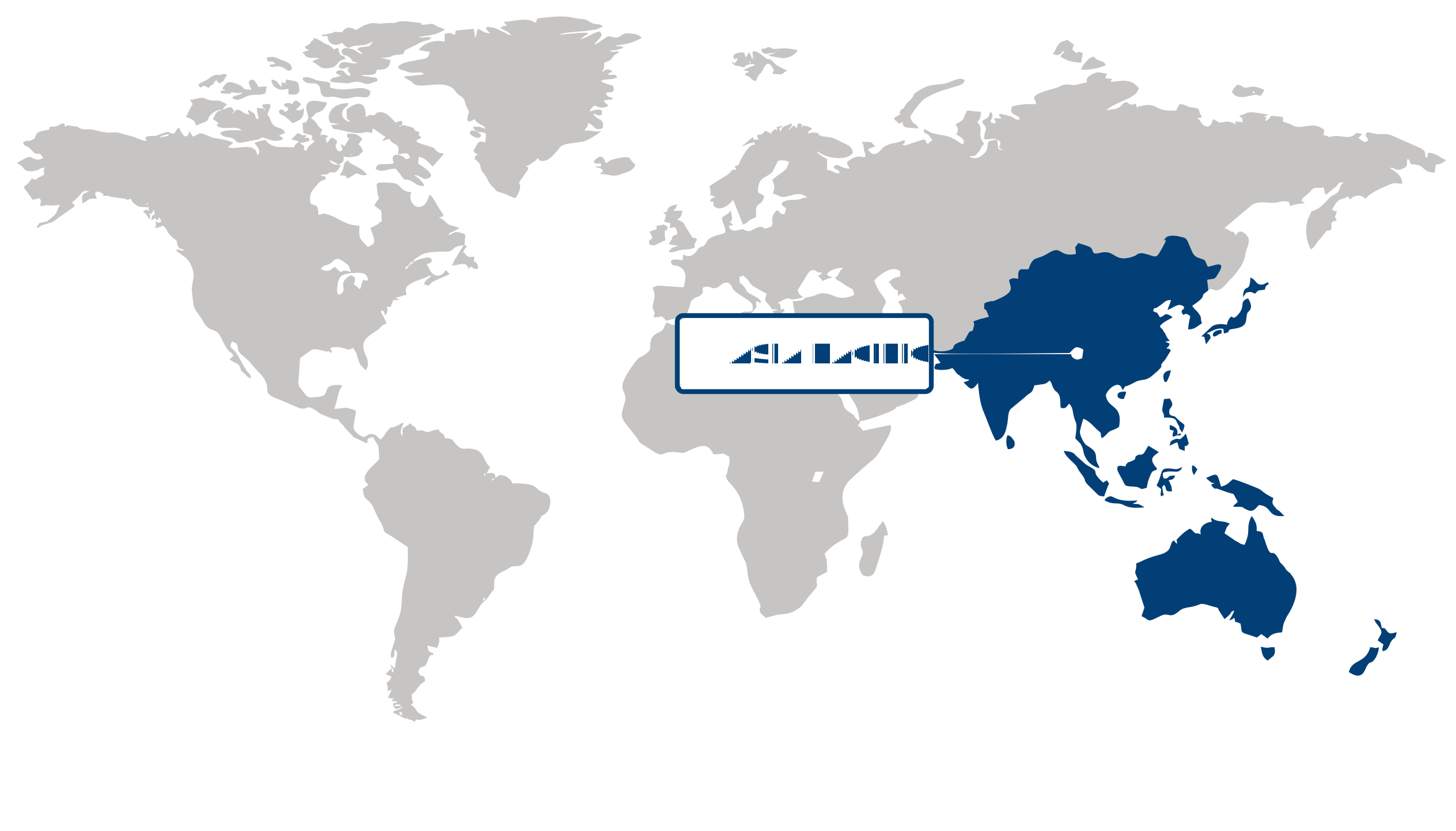
Asia Pacific (Largest Region)
The extreme ultraviolet lithography market was led by
North America (Fastest-Growing Region)
Asia Pacific, which represented a 66.31% share in 2026, supported by the region's concentration of advanced semiconductor manufacturing, extensive investment in fabrication capacity, and strong demand for increasingly sophisticated chip architectures. The push toward smaller process geometries and higher-performance semiconductor devices is reinforcing the need for advanced lithography capabilities, while established electronics supply chains and semiconductor research infrastructure provide a strong foundation for technology deployment. Continued investment in fabrication facilities and the strategic importance of domestic semiconductor production are further strengthening regional demand. North America is the fastest-growing regional market as semiconductor capacity expansion, technology development, and efforts to strengthen domestic chip manufacturing increase the strategic importance of advanced lithography systems. Rising investment in semiconductor infrastructure and research is encouraging greater adoption of next-generation manufacturing technologies, while demand for high-performance processors across computing, artificial intelligence, and other advanced applications is supporting the expansion of the regional semiconductor ecosystem.
| Parameter | North America | Asia Pacific | Europe | Latin America | MEA |
|---|---|---|---|---|---|
| Innovation Hub i Scale Nascent Developing Advanced | |||||
| Cost-Sensitive Region i Scale Low Medium High | |||||
| Regulatory Environment i Scale Restrictive Neutral Supportive | |||||
| Demand Drivers i Scale Weak Moderate Strong | |||||
| Development Stage i Scale Emerging Developing Developed | |||||
| Adoption Rate i Scale Low Medium High | |||||
| New Entrants / Startups i Scale Sparse Moderate Dense | |||||
| Macro Indicators i Scale Weak Stable Strong |
Key Country Insights
Germany 🇩🇪
Precision equipment engineering baseGermany plays a key role in precision engineering and advanced optics within the semiconductor equipment supply chain. In Germany, extreme ultraviolet lithography development and supporting subsystems benefit from strong mechanical engineering expertise, enabling high-precision components, vibration control systems, and materials innovation critical to sustaining next-generation lithography performance.
France 🇫🇷
Research-led semiconductor participationFrance focuses on research-driven contributions to the semiconductor ecosystem, particularly through advanced materials research and pilot-line development. In France, extreme ultraviolet lithography activity is concentrated in collaborative R&D programs and early-stage technology validation, supporting broader European semiconductor innovation initiatives and scaling research infrastructure capabilities.
Italy 🇮🇹
Niche semiconductor adoptionItaly participates in selective semiconductor research and industrial technology programs, with extreme ultraviolet lithography engagement largely concentrated in research institutions and specialized equipment supply chain roles. In Italy, development efforts emphasize precision manufacturing components and collaborative European semiconductor initiatives, supporting incremental adoption pathways.
Japan 🇯🇵
Advanced photonics manufacturing integrationJapan emphasizes advanced materials science and photonics integration within the semiconductor manufacturing ecosystem. In Japan, extreme ultraviolet lithography adoption is supported by precision optics, photoresist innovation, and high-purity materials, enabling tighter process control and improved patterning performance in leading-edge semiconductor fabrication environments.
South Korea 🇰🇷
Memory-driven lithography demandSouth Korea is a major hub for advanced memory semiconductor production, where EUV lithography is increasingly applied to DRAM and NAND scaling. In South Korea, demand is driven by high-volume manufacturing efficiency requirements, process yield optimization, and continuous node shrink efforts across leading memory fabrication facilities.
United States 🇺🇸
Semiconductor scaling leadership ecosystemsThe United States market is driven by advanced semiconductor design leadership and strong ecosystem coordination between fabless firms, equipment suppliers, and foundry partners. In the United States, extreme ultraviolet lithography is central to next-generation node scaling efforts, supporting advanced chip manufacturing for AI, high-performance computing, and data center applications.
Segment Leadership and Growth Trends
Extreme Ultraviolet Lithography Market Share (%), by End Use, 2026
Go beyond the chart, access full insights & data tables
Request Free Sample ReportEnd Use Segment Analysis: Integrated Device Manufacturer (IDM) (Largest Segment) vs Foundries (Fastest-Growing Segment)
Integrated device manufacturer (IDM) held the largest share of the extreme ultraviolet lithography market, accounting for 61.98% share in 2026. IDMs benefit from greater control over semiconductor design and manufacturing, making advanced lithography capabilities strategically important for producing increasingly sophisticated chips. The growing need for precise patterning at advanced process nodes, along with continued investment in high-performance semiconductor manufacturing, supports strong demand from this end-use segment.
Foundries represent the fastest-growing end-use segment as semiconductor manufacturers increasingly expand specialized production capabilities to serve diverse chip designers. Rising demand for advanced-node fabrication, increasing complexity in semiconductor architectures, and the need for highly precise lithography are encouraging foundries to adopt extreme ultraviolet technology to improve manufacturing capabilities and address increasingly demanding production requirements.
Equipment Segment Analysis: Light Source (Largest Segment) vs Mask (Fastest-Growing Segment)
The light source segment dominated the extreme ultraviolet lithography market with a 42.51% share in 2026, reflecting its fundamental role in enabling extremely precise semiconductor patterning. The performance of the light source directly influences lithography quality, process efficiency, and the ability to support advanced manufacturing requirements, making continued technological development in this equipment category essential to the evolution of EUV production systems.
The mask segment is the fastest-growing equipment category as semiconductor fabrication increasingly requires highly sophisticated pattern-transfer components capable of supporting advanced chip designs. Growing pattern complexity and the continued push toward smaller and more densely integrated semiconductor features are increasing the importance of mask precision, quality, and compatibility with advanced EUV manufacturing processes.
| Segment | Sub-Segment | Largest Segment | Fastest Growing |
|---|---|---|---|
| End Use | Integrated Device Manufacturer (IDM), Foundries | Integrated Device Manufacturer (IDM) | Foundries |
| Equipment | Light Source, Optics, Mask, Others | Light Source | Mask |
Competitive Landscape and Market Positioning
Top players in the extreme ultraviolet lithography market:
1. ASML Holding N.V. (Netherlands)
2. Taiwan Semiconductor Manufacturing Company Limited (Taiwan)
3. Samsung Electronics Co. Ltd. (South Korea)
4. Intel Corporation (United States)
5. Nikon Corporation (Japan)
6. Canon Inc. (Japan)
7. ZEISS Group (Germany)
8. Tokyo Electron Limited (Japan)
9. Toppan Photomasks Inc. (Japan)
10. Ushio Inc. (Japan)
The extreme ultraviolet lithography market is progressing as semiconductor manufacturing moves toward smaller node architectures. Precision engineering improvements are enhancing pattern resolution and production efficiency. Collaborative development efforts are supporting next-generation chip fabrication capabilities essential for advanced computing applications.
| Company | Market Share | Company Revenue | Revenue CAGR (%) | Product Portfolio | Geographic Presence | Innovation / R&D Focus | Strategic Developments |
|---|---|---|---|---|---|---|---|
| ASML Holding N.V. (Netherlands) | |||||||
| Taiwan Semiconductor Manufacturing Company Limited (Taiwan) | |||||||
| Samsung Electronics Co. Ltd. (South Korea) | |||||||
| Intel Corporation (United States) | |||||||
| Nikon Corporation (Japan) | |||||||
| Canon Inc. (Japan) | |||||||
| ZEISS Group (Germany) | |||||||
| Tokyo Electron Limited (Japan) | |||||||
| Toppan Photomasks Inc. (Japan) | |||||||
| Ushio Inc. (Japan). |
Industry Development/News
| Company Name | Date | Key Development |
|---|---|---|
| ASML | May-26 | ASML has entered a strategic agreement to supply advanced lithography systems and technical expertise to Tata Electronics for its $11 billion semiconductor fab in Dholera, India. This collaboration is pivotal for establishing India's first major front-end semiconductor manufacturing facility and reinforces ASML’s position in expanding global next-generation chip production infrastructure and ecosystem readiness. |
| Samsung Electronics | Jan-26 | Samsung Electronics is initiating test operations of EUV lithography equipment at its Taylor, Texas facility. This operational milestone is critical for the upcoming full-scale production scheduled for the second half of 2026, intended to support advanced AI and autonomous driving chip fabrication, thereby significantly enhancing the company’s advanced-node manufacturing footprint within the United States. |
| AlixLabs AB | Nov-25 | AlixLabs AB secured approximately $16.2 million in funding to commercialize semiconductor manufacturing technologies focused on cost-efficient, leading-edge chip production. The capital supports the development of advanced patterning techniques designed as viable alternatives or complements to traditional EUV-dependent scaling, potentially impacting the cost structure and technological requirements of future high-density semiconductor fabrication processes. |
| Intel | Oct-25 | Intel has expanded its procurement of High-NA EUV lithography systems from ASML to accelerate its advanced process roadmap. By increasing its adoption of these tools, Intel aims to strengthen its foundry capabilities and improve its competitive positioning in the high-performance computing and AI semiconductor markets through enhanced manufacturing precision at leading-edge nodes. |
| Xanadu; Mitsubishi Chemical | Jul-25 | Xanadu and Mitsubishi Chemical have launched a collaborative project to develop quantum algorithms for optimizing EUV lithography processes. By applying quantum machine learning to semiconductor manufacturing, the partnership seeks to improve precision and process control, potentially offering a transformative approach to enhancing efficiency and throughput in complex EUV-based chip production environments. |
| Huawei | May-25 | Huawei is actively advancing an alternative lithography approach to facilitate semiconductor scaling despite ongoing export restrictions on ASML’s EUV systems. This initiative represents a strategic effort to decouple from Western manufacturing equipment and build independent domestic capacity for sub-7nm and advanced-node chip production, targeting critical high-performance and AI-driven applications. |
| TSMC | Apr-25 | TSMC has indicated that its upcoming A14 (1.4nm) process node will not initially utilize High-NA EUV lithography equipment. This strategic decision highlights a focus on process optimization and cost management, signaling a selective approach to adopting next-generation lithography tools while prioritizing the balance between manufacturing complexity and yield efficiency at the leading edge of semiconductor production. |
| ZEISS Group | Jan-24 | ZEISS Group introduced its High-NA (Numerical Aperture) EUV lithography system, marking a significant advancement in semiconductor manufacturing technology. The system enables the production of microchips with significantly finer features compared to legacy EUV equipment, directly facilitating the scaling required for next-generation logic and memory devices and establishing a new technical benchmark for the semiconductor industry. |
Customize Your Report
Explore examples of how this report can be tailored to different research needs, including custom segments, additional topics or chapters, and related reports. Click a section of the wheel or its numbered marker to explore the available options.
Extreme Ultraviolet Lithography Market — Custom Segments
| Segment | Sub-Segment |
|---|---|
| Semiconductor Node | 7 nm and Above, 5 nm, 3 nm, 2 nm and Below |
| Numerical Aperture Generation | Low-NA EUV, High-NA EUV |
| Production Stage | Research & Development, Pilot Production, High-Volume Manufacturing |
Extreme Ultraviolet Lithography Market — Custom TOC
| Custom Chapter | Custom Details |
|---|---|
| Semiconductor Manufacturing Roadmap Analysis |
|
| EUV Adoption Barrier Assessment |
|
| Fab Investment and Expansion Outlook |
|
Need a different cut of the data?
Request Custom ResearchWhat is the current size of the extreme ultraviolet lithography market?
What are the growth projections for the extreme ultraviolet lithography industry?
Why is AI and 5G semiconductor scaling accelerating EUV lithography adoption?
How are semiconductor fab investments influencing EUV market expansion?
Why do integrated device manufacturers (IDMs) lead the extreme ultraviolet lithography market?
Why is the mask segment the fastest-growing equipment category in the extreme ultraviolet lithography market?
Why is Asia Pacific the largest market for extreme ultraviolet lithography?
What is accelerating EUV lithography market growth in North America?
Who are the leading players in the extreme ultraviolet lithography landscape?
Our Clients
"Working with FBI has been a good experience. The market report provided a holistic view, covering everything from emerging trends to potential risks."
Semtech Corporation
"The experience was highly positive. The team showcased remarkable flexibility in adapting to our specific needs and delivered report that perfectly aligned with all our requirements."
TSMC
"What really stood out to me was how clearly and promptly the Fundamental Business Insights team communicated throughout. It made the collaboration feel effortless."
NXP Semiconductors
Our Research Team & Methodology
Every Fundamental Business Insights report is built by a dedicated vertical research team, validated through a structured primary-and-secondary methodology, and reviewed for accuracy before it reaches you.
Research Team Overview
Prepared by the Electronics & Semiconductors Research Team
Delivery
Published
Demand
Available
Support
Trust & Compliance
Research Domains
10 coverage areasResearch Intelligence
| Source | Reference |
|---|---|
| Semiconductor Industry Association (SIA) | www.semiconductors.org |
| SEMI | www.semi.org |
| JEDEC Solid State Technology Association | www.jedec.org |
| IEEE | www.ieee.org |
| IPC – Association Connecting Electronics Industries | www.ipc.org |
| International Electrotechnical Commission (IEC) | www.iec.ch |
| International Organization for Standardization (ISO) | www.iso.org |
| U.S. Bureau of Industry and Security (BIS) | www.bis.gov |
| U.S. Patent and Trademark Office (USPTO) | www.uspto.gov |
| European Patent Office (EPO) | www.epo.org |
| Taiwan Semiconductor Industry Association (TSIA) | www.tsia.org.tw |
| World Semiconductor Trade Statistics (WSTS) | www.wsts.org |
| International Energy Agency (IEA) | www.iea.org |
| GSMA | www.gsma.com |
| 3GPP | www.3gpp.org |
| ITU (International Telecommunication Union) | www.itu.int |
| Omdia (public insights) | omdia.tech.informa.com |
| Display Supply Chain Consultants (DSCC) | www.displaysupplychain.com |
| U.S. Department of Energy (DOE) | www.energy.gov |
| NIST (National Institute of Standards and Technology) | www.nist.gov |
Research Workflow & Quality Assurance
Data Collection
Verified information gathered through primary and secondary research.
Data Triangulation
Cross-validation using multiple independent data sources.
Forecast Modelling
Market estimates developed using historical trends and analytical models.
Analyst Validation
Findings reviewed by domain experts for accuracy and consistency.
Editorial & Quality Review
Final editorial, quality, and compliance checks before publication.
Final Publication
Released after successful completion of the internal review process.
Report Coverage
📊 Market Assessment
- Market Size & Forecast
- Market Segmentation
- Regional Analysis
- Growth Drivers & Challenges
- Market Dynamics
🏢 Competitive Intelligence
- Competitive Landscape
- Company Profiles
- Competitive Benchmarking
- Mergers & Acquisitions
- Market Share Analysis or Key Company Strategies
🔍 Strategic Analysis
- Value Chain Analysis
- Porter's Five Forces
- PESTLE Analysis
- Pricing Trends
- Supply-Demand Analysis
🚀 Future Outlook
- Technology Landscape
- Regulatory Landscape
- Investment & Funding Landscape
- Emerging Opportunities
- Future Market Outlook
Have a question about this report or need a custom scope?
Request Customization