CMP Slurry Market Size & Forecasts 2026-2035, By Segments (Type, Application), Growth Opportunities, Innovation Landscape, Regulatory Shifts, Strategic Regional Insights (U.S., Japan, China, South Korea, UK, Germany, France), and Competitive Dynamics (Cabot Microelectronics, Fujimi Incorporated, Ebara Corporation, Dow Inc., Hitachi Chemical)
Market Size and Growth Outlook
CMP Slurry Market size is anticipated to rise from USD 2.09 billion in 2025 to USD 4.73 billion by 2035, reflecting a CAGR surpassing 8.5% over the forecast horizon of 2026-2035. The estimated revenue for 2026 is USD 2.25 billion.
Get more details on this report
Request Free Sample ReportCMP Slurry Market Intelligence Snapshot
Regional Market Dynamics
Segment Momentum
Market Expansion Drivers
Leading Market Participants
Global Market Forecast Snapshot
Market Outlook
Regional and Segment Outlook
Market Growth Drivers and Industry Trends
Advanced wafer fabrication technology adoption: Widespread deployment of EUV lithography and complex multi-material stacks—documented in ASML equipment shipments and research by IMEC and in process tool roadmaps from Applied Materials and Lam Research—raises polishing precision and compatibility requirements for the CMP slurry market. New materials (metal gates, low-k dielectrics) and tighter defect budgets compel collaborative development between fabs and slurry formulators, as seen in co-development announcements by leading toolmakers. Incumbents can capitalize by co-engineering tailored chemistries and offering integrated metrology services; challengers can differentiate with novel chemistries and analytical capabilities. Observable tool adoption and published technology roadmaps indicate growing demand for application-specific slurries and faster R&D cycles.
Expansion of green semiconductor initiatives: Policy actions such as the U.S. CHIPS and Science Act and the European Commission’s Green Deal, together with sustainability pledges from Intel and TSMC, are redirecting fab procurement toward lower-waste and lower-toxicity processes, affecting the CMP slurry market. Programs run by the U.S. Department of Energy and industry guidance from SEMI emphasize water reuse and chemical footprint reduction, encouraging development of biodegradable formulations and closed-loop rinse systems. Large suppliers can retrofit offerings to meet compliance and lifecycle reporting needs; startups can pursue green chemistry and recycling services as entry points. As public funding and corporate net‑zero targets remain active, environmental performance will become a procurement differentiator for slurries.
Industry Restraints:
Raw Material and Supply Chain Vulnerabilities
CMP slurry performance depends on tightly specified abrasives and chemistries (ceria, colloidal silica, oxidizers) that are produced in concentrated geographies and by a small set of suppliers; disruptions therefore throttle tool uptime and supplier qualification cycles. The Semiconductor Industry Association (SIA) and the U.S. Bureau of Industry and Security (BIS) have documented how geographic concentration and export controls create chokepoints for materials and advanced process inputs, while suppliers such as Cabot Microelectronics, Fujimi, and Merck KGaA are frequently cited as dominant upstream players. For incumbents this drives inventory hedging, long-term contracts, and selective vertical integration; for new entrants it raises capital and qualification barriers. Expect continued supply-driven allocation dynamics and strategic localization efforts to shape procurement and partner selection in the near to medium term.
Regulatory and Environmental Compliance Burdens
Emerging regulatory scrutiny of nanoparticles, effluents, and chemical constituents increases compliance complexity and operating costs across slurry production and semiconductor fabs. The European Chemicals Agency (ECHA) under REACH has intensified assessment of nanomaterials, the U.S. Environmental Protection Agency (EPA) enforces Clean Water Act/NPDES requirements for wastewater streams, and China’s Ministry of Ecology and Environment (MEE) has tightened discharge standards—each raising permitting timelines and treatment capital needs. Companies with established compliance infrastructure (for example, Merck KGaA and Cabot Microelectronics) can absorb or pass through costs more readily; smaller entrants face longer approval cycles and higher upfront investment. This regulatory pressure is likely to sustain higher barriers to entry and push portfolio reformulation and consolidation over the near to medium term.
| Growth Driver | Impact on CAGR | Regulatory Influence | Geographic Relevance | Adoption Rate | Impact Timeline |
|---|---|---|---|---|---|
| Semiconductor device production growth | 2.00% | Short term (≤ 2 yrs) | Asia Pacific, North America; Spillover: Europe | Medium | Fast |
| Advanced wafer fabrication technology adoption | 1.80% | Medium term (2–5 yrs) | North America, Asia Pacific; Spillover: Europe | Medium | Moderate |
| Expansion of green semiconductor initiatives | 1.20% | Long term (5+ yrs) | Europe, Asia Pacific; Spillover: North America | High | Slow |
Unlock insights tailored to your business with our bespoke market research solutions.
Click to get your customized report now.
Regional Demand Dynamics
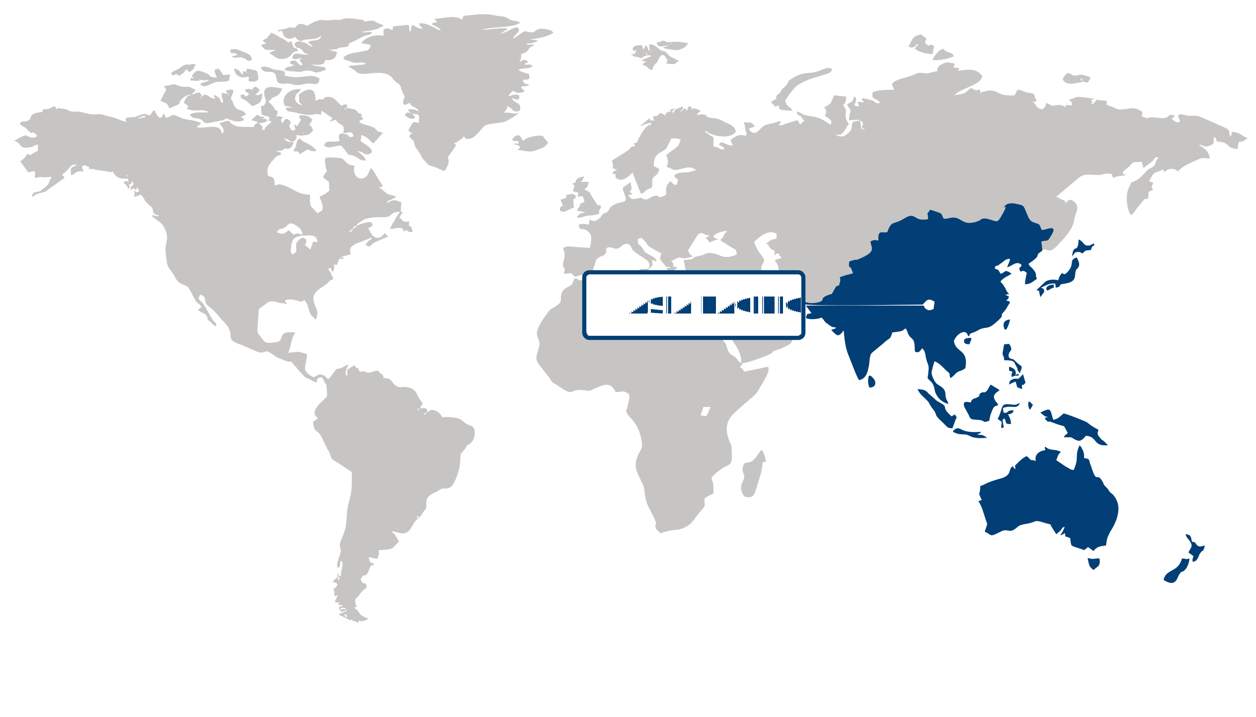
CMP slurry market in Asia Pacific captured approximately 49.00% of the global market in 2025, making the region the largest center for slurry demand. This leadership is underpinned by strong semiconductor fabrication and foundry capacity expansion across Taiwan, South Korea, China and Japan, with capacity commitments and roadmap updates from Taiwan Semiconductor Manufacturing Company (TSMC) and Samsung Electronics reinforcing rising wafer starts (TSMC press release; Samsung Electronics press release). Announcements from the Ministry of Industry and Information Technology and Japan’s Ministry of Economy, Trade and Industry have further aligned investment and industrial support, accelerating demand for higher-performance, lower-defectivity chemistries and closer technical partnerships. Given these structural drivers, Asia Pacific offers sizable opportunities in specialty formulations, localized supply-chain investments, and integrated on-site services tied to advanced-node manufacturing needs.
CMP slurry market in Japan is positioned as a pivotal hub in Asia Pacific, supplying high-purity chemistries and precision R&D that serve advanced fabs. Domestic materials leaders such as JSR Corporation and Fujimi Corporation have publicly signaled expanded R&D and new product initiatives to meet stricter defectivity and uniformity requirements (JSR Corporation press release; Fujimi Corporation press release), while Shin-Etsu Chemical’s materials footprint continues to support wafer fabrication ecosystems. Coordination with Japan’s Ministry of Economy, Trade and Industry has encouraged industry–producer collaboration and capital deployment. Strategically, Japan’s concentration of specialty suppliers and engineering capability makes it a prime partner for foundries seeking premium, high-reliability CMP solutions across the region.
CMP slurry market in China anchors the region’s capacity expansion through rapid scaling of domestic foundries and higher local wafer demand. Semiconductor Manufacturing International Corporation (SMIC) capacity announcements and guidance from the Ministry of Industry and Information Technology illustrate a push toward greater domestic production and wafer starts (SMIC press release; Ministry of Industry and Information Technology announcements), creating large-volume requirements for cost-competitive slurries. Local chemical manufacturers are accelerating qualification cycles and collaborating directly with foundries to capture volume business and shorten delivery timelines. For suppliers and investors, China presents scale-driven opportunities in high-throughput manufacturing, localization of supply chains, and service models tailored to large foundry operations.
North America Market Analysis:
North America emerged as the fastest-growing region in the CMP slurry market, registering a robust CAGR of 10.2% driven by increasing investments in advanced semiconductor manufacturing. Major public and private initiatives—most notably funding enabled by the U.S. Department of Commerce under the CHIPS and Science Act and large-scale capacity commitments from Intel Corporation and TSMC—are expanding wafer fabrication activity, raising demand for high-specification slurry formulations and tighter supply-chain coordination. Buyers increasingly prioritize process consistency, lower-defect yields and environmental compliance, prompting suppliers to scale technical service teams and reformulate chemistries. Announcements from Intel Corporation, TSMC and Micron Technology illustrate near-term order flows and qualification programs. Given sustained capital deployment and policy support, North America offers concentrated commercial opportunity for premium CMP slurry suppliers and co-development partnerships.
The U.S. plays the central role in the CMP slurry market within North America, where federal incentives and domestic fabs uniquely accelerate adoption and qualification cycles. U.S. actions—evidenced by Department of Commerce CHIPS-related grants and facility commitments from Intel Corporation in Ohio, TSMC in Arizona and Micron Technology in New York—create immediate demand for qualified slurry volumes, localized technical support and shortened qualification timelines. Suppliers able to align manufacturing footprint, environmental permitting and rapid on-site process engineering win placement as fabs ramp. Strategic implication: securing U.S. fab partnerships and supply-chain resilience positions vendors to capture the broader North American growth tied to advanced-node capacity build-outs.
Europe Market Trends:
The CMP slurry market in Europe maintained a notable presence and is viewed as high potential as EU-level funding and localized fab builds accelerate demand for consumables and specialty chemicals. European Commission actions under the EU Chips Act and targeted financing from the European Investment Bank have catalyzed capacity expansions across the region, while suppliers such as Merck KGaA and Cabot Microelectronics have highlighted Europe-focused investments and partnerships in recent press releases. These developments intersect with stronger sustainability expectations, tighter supply-chain sourcing, and advanced-node adoption, creating sustained procurement needs for high-performance slurries and slashing logistics lead times. Together, policy momentum and supplier commitments make Europe a strategic market for slurry product differentiation and nearshoring of supply.
Germany plays a leading role in the CMP slurry market as its concentration of power- and automotive-semiconductor manufacturing underpins steady, higher-spec consumption of planarization chemistries. Announcements from Infineon Technologies about capacity investments and support measures from the German Federal Ministry for Economic Affairs and Climate Action have signaled durable domestic demand for wafer-level consumables; at the same time Merck KGaA’s materials investments in Germany underscore local supply capabilities. For slurry suppliers, Germany’s engineering talent base and OEM-driven specifications create opportunities for co-development, qualification programs, and long-term supply agreements that reinforce regional supply-chain resilience.
France is an important growth market in the CMP slurry market as government-backed industrial programs and research collaborations accelerate fab projects and advanced-material adoption. The French government’s France 2030 initiative, together with manufacturing and R&D activity from STMicroelectronics and research partnerships with CEA-Leti, has stimulated upstream demand for precision process chemistries and closer supplier integration. These policy-backed investments and cluster-level innovation mean slurry vendors can leverage pilot lines and joint qualification with local fabs to shorten time-to-market and capture share as France’s semiconductor ecosystem scales.
| Parameter | North America | Asia Pacific | Europe | Latin America | MEA |
|---|---|---|---|---|---|
| Innovation Hub i Scale Nascent Developing Advanced | |||||
| Cost-Sensitive Region i Scale Low Medium High | |||||
| Regulatory Environment i Scale Restrictive Neutral Supportive | |||||
| Demand Drivers i Scale Weak Moderate Strong | |||||
| Development Stage i Scale Emerging Developing Developed | |||||
| Adoption Rate i Scale Low Medium High | |||||
| New Entrants / Startups i Scale Sparse Moderate Dense | |||||
| Macro Indicators i Scale Weak Stable Strong |
Segment Leadership and Growth Trends
CMP Slurry Market Share (%), by Type, 2026
Go beyond the chart, access full insights & data tables
Request Free Sample ReportSilica CMP Slurry dominated the CMP slurry market as the largest share in 2025, driven by its extensive use in advanced semiconductor planarization processes. This segment leads because silica-based chemistries deliver the repeatable oxide and dielectric removal rates required by leading fabs, a performance emphasis highlighted in Applied Materials and Lam Research materials and application notes; Intel’s published process roadmaps also underscore stringent planarization needs at advanced nodes. Fabricators’ preference for process stability, tighter supplier SLAs, and sustainability-led formulation improvements have strengthened supply-chain partnerships around silica segments, creating opportunities for established chemical suppliers to bundle services and for agile entrants to offer green, niche formulations. Given ongoing node scaling and advanced packaging demands, silica segments are positioned to remain central to wafer-level planarization in the near to medium term.
Analysis by Application
Silicon Wafers represented largest share in the CMP slurry market in 2025, propelled by increasing production of integrated circuits and semiconductor devices. High-volume wafer fabrication at foundries such as TSMC, Samsung Electronics, and Intel drives sustained slurry consumption, a trend corroborated by SEMI industry commentary and capacity expansion announcements; policy drivers like the U.S. CHIPS and Science Act have further accelerated onshoring and local sourcing. Fabricator demand patterns favor suppliers that provide consistent lot-to-lot performance, digital process control integration, and localized logistics, elevating the strategic value of wafer-focused segments for legacy suppliers and lean startups offering advanced process control or eco-friendly chemistries. With continued IC demand, node refinement, and packaging complexity, silicon wafer-related segments will remain strategically relevant through the near to medium term.
| Segment | Sub-Segment | Largest Segment | Fastest Growing |
|---|---|---|---|
| Type | Aluminum Oxide CMP Slurry, Cerium Oxide CMP Slurry, Ceramic CMP Slurry, Silica CMP Slurry | ||
| Application | Silicon Wafers, Disk-Drive Components, Optical Substrates, Others, DIY Activities |
Competitive Landscape and Market Positioning
The competitive landscape reflects intensified differentiation through expanded product breadth, closer customer alignment, and accelerated development capability. Several firms have integrated complementary portfolios and deepened co-development with device manufacturers, while others have prioritized next-generation chemistries and increased pilot-scale capacity to shorten qualification cycles. Enhanced technical-service footprints and regional production points have tightened customer relationships, enabling bespoke slurries for advanced materials and multi-layer stacks. These moves reinforce incumbent advantages around reliability and customization, raise the bar for new entrants, and shift competition toward speed of adaptation and application expertise rather than commodity positioning.
Strategic / Actionable Recommendations for Regional Players
North America: Focus on tighter alignment with local logic, MEMS and compound-semiconductor fabs by expanding joint development and pilot offerings, while augmenting analytics- and AI-enabled process support to reduce time-to-qualification. Increasing onshore pilot capacity and a responsive technical-service organization will help capture high-margin, low-volume advanced-node work and counter large global suppliers’ scale advantages.
Asia Pacific: Prioritize closer co-development with high-volume foundries and regional IDMs, scale localized manufacturing to ensure supply continuity, and tailor formulations for both mature and advanced process nodes common in the region. Strengthening in-region application labs and training programs will accelerate adoption and create differentiation through service-led value.
Europe: Leverage strong specialty-chemistry and sustainability expertise to serve automotive- and industrial-oriented semiconductor segments, collaborate more tightly with equipment and materials partners for system-level compatibility, and emphasize environmentally compliant, low-impact formulations. Building modular customization capabilities and lifecycle support will appeal to customers seeking regulatory alignment and long-term supply partnerships.
| Company | Market Share | Company Revenue | Revenue CAGR (%) | Product Portfolio | Geographic Presence | Innovation / R&D Focus | Strategic Developments |
|---|---|---|---|---|---|---|---|
| No companies available. | |||||||
Industry Development/News
| Company Name | Date | Key Development |
|---|
Customize Your Report
Explore examples of how this report can be tailored to different research needs, including custom segments, additional topics or chapters, and related reports. Click a section of the wheel or its numbered marker to explore the available options.
CMP Slurry Market — Custom Segments
| Segment | Sub-Segment |
|---|---|
| No segment data available. | |
CMP Slurry Market — Custom TOC
| Custom Chapter | Custom Details | ||
|---|---|---|---|
| No custom TOC data available. | |||
Need a different cut of the data?
Request Custom ResearchHow large is the CMP slurry market?
What is the anticipated CAGR of the CMP slurry industry?
Which part of the world represents the largest segment of the CMP slurry market?
What region has posted the highest CAGR in the CMP slurry sector?
Which is the largest sub-segment within the type segment for CMP slurry industry?
Why does silicon wafers sub-segment dominate the application segment of CMP slurry sector?
Who holds a significant market share in the CMP slurry landscape?
Our Clients
"Working with FBI has been a good experience. The market report provided a holistic view, covering everything from emerging trends to potential risks."
Semtech Corporation
"The experience was highly positive. The team showcased remarkable flexibility in adapting to our specific needs and delivered report that perfectly aligned with all our requirements."
TSMC
"What really stood out to me was how clearly and promptly the Fundamental Business Insights team communicated throughout. It made the collaboration feel effortless."
NXP Semiconductors
Our Research Team & Methodology
Every Fundamental Business Insights report is built by a dedicated vertical research team, validated through a structured primary-and-secondary methodology, and reviewed for accuracy before it reaches you.
Research Team Overview
Prepared by the Electronics & Semiconductors Research Team
Delivery
Published
Demand
Available
Support
Trust & Compliance
Research Domains
10 coverage areasResearch Intelligence
| Source | Reference |
|---|---|
| Semiconductor Industry Association (SIA) | www.semiconductors.org |
| SEMI | www.semi.org |
| JEDEC Solid State Technology Association | www.jedec.org |
| IEEE | www.ieee.org |
| IPC – Association Connecting Electronics Industries | www.ipc.org |
| International Electrotechnical Commission (IEC) | www.iec.ch |
| International Organization for Standardization (ISO) | www.iso.org |
| U.S. Bureau of Industry and Security (BIS) | www.bis.gov |
| U.S. Patent and Trademark Office (USPTO) | www.uspto.gov |
| European Patent Office (EPO) | www.epo.org |
| Taiwan Semiconductor Industry Association (TSIA) | www.tsia.org.tw |
| World Semiconductor Trade Statistics (WSTS) | www.wsts.org |
| International Energy Agency (IEA) | www.iea.org |
| GSMA | www.gsma.com |
| 3GPP | www.3gpp.org |
| ITU (International Telecommunication Union) | www.itu.int |
| Omdia (public insights) | omdia.tech.informa.com |
| Display Supply Chain Consultants (DSCC) | www.displaysupplychain.com |
| U.S. Department of Energy (DOE) | www.energy.gov |
| NIST (National Institute of Standards and Technology) | www.nist.gov |
Research Workflow & Quality Assurance
Data Collection
Verified information gathered through primary and secondary research.
Data Triangulation
Cross-validation using multiple independent data sources.
Forecast Modelling
Market estimates developed using historical trends and analytical models.
Analyst Validation
Findings reviewed by domain experts for accuracy and consistency.
Editorial & Quality Review
Final editorial, quality, and compliance checks before publication.
Final Publication
Released after successful completion of the internal review process.
Report Coverage
📊 Market Assessment
- Market Size & Forecast
- Market Segmentation
- Regional Analysis
- Growth Drivers & Challenges
- Market Dynamics
🏢 Competitive Intelligence
- Competitive Landscape
- Company Profiles
- Competitive Benchmarking
- Mergers & Acquisitions
- Market Share Analysis or Key Company Strategies
🔍 Strategic Analysis
- Value Chain Analysis
- Porter's Five Forces
- PESTLE Analysis
- Pricing Trends
- Supply-Demand Analysis
🚀 Future Outlook
- Technology Landscape
- Regulatory Landscape
- Investment & Funding Landscape
- Emerging Opportunities
- Future Market Outlook
Have a question about this report or need a custom scope?
Request Customization